Choosing the Right Easy PCB Maker for Your Project
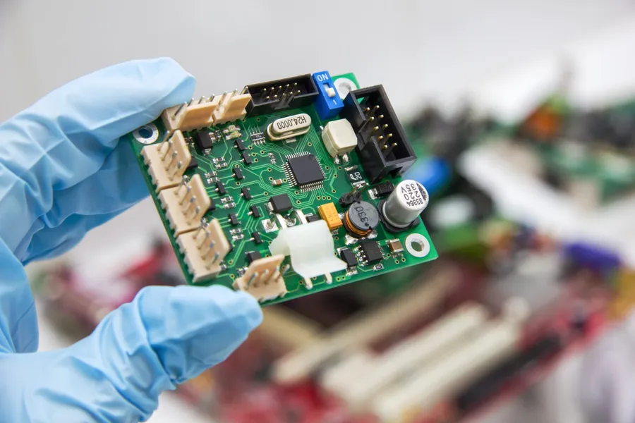
In today's world, electronics are woven into the fabric of our daily lives, from smartphones to smart homes. Creating custom circuit boards is no longer exclusive to engineers, thanks to the rise of easy PCB makers. Whether you're a hobbyist or a seasoned professional, this article will guide you through selecting the best PCB design software to transform your electronic ideas into physical reality. These tools bridge the gap between imagination and fabrication, enabling both simple and complex projects.
Understanding the Needs of an Easy PCB Maker
An 'easy' PCB maker is characterized by its user-friendliness, which extends beyond a simple interface to include intuitive workflows, comprehensive component libraries, and robust feature sets for schematic capture, PCB layout, and simulation. The primary goal is to lower the barrier to entry for beginners while providing the necessary power for experienced designers to complete their projects quickly and efficiently.
At the heart of this task is the need to define 'easy' within the context of PCB design software. The user's intent is to find a tool that is both accessible and capable of producing professional results. Key information needed includes the user's skill level, project complexity, budget constraints, and desired features. Possible solutions include online platforms, free desktop software, or commercial-grade tools with trial periods, each with its own set of advantages and disadvantages.
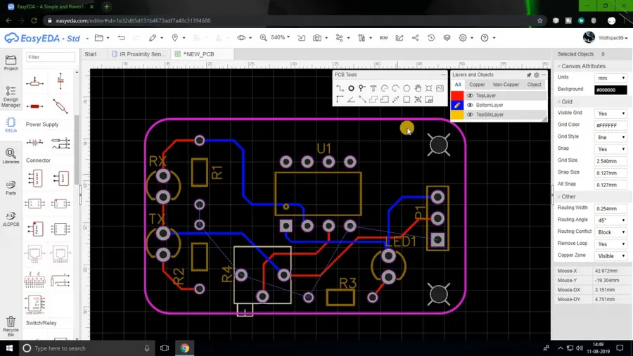
Top Free Online PCB Design Tools
Web-based PCB design tools offer a compelling alternative to traditional desktop software, providing accessibility and convenience for designers. These platforms, accessible through any internet-connected device, typically emphasize user-friendliness, making them ideal for beginners and collaborative projects.
This section focuses on prominent free online PCB design tools, assessing their capabilities, ease of use, and suitability for various project needs.
| Feature | EasyEDA | Other Online Tools |
|---|---|---|
| Integrated Environment | Offers schematic capture, PCB layout, and simulation within a single platform. | May require using multiple tools from various providers. |
| Ease of Use | Designed with an intuitive interface, making it easy for beginners to start quickly. | Varies by platform, some might be complex and others extremely simple. |
| Accessibility | Accessible from any device with a web browser and internet connection. | Limited to web browser usage. |
| Component Libraries | Extensive component libraries that are often user-updated and maintained. | Often a more limited database compared to paid options. |
| Simulation Capabilities | Provides basic simulation tools for circuit testing and analysis. | Vary in terms of capabilities or may not be included in free online tools. |
| Collaboration Features | Supports real-time project collaboration amongst team members. | Not always available or might require a paid plan. |
| Project Storage | Stores project in the cloud with limited free storage. | Project storage can be limited or have a pay for service |
| File Export Options | Supports exporting to Gerber, DXF and other formats to allow for fabrication. | File formats may be limited to specific standards. |
Free Software Options for PCB Design
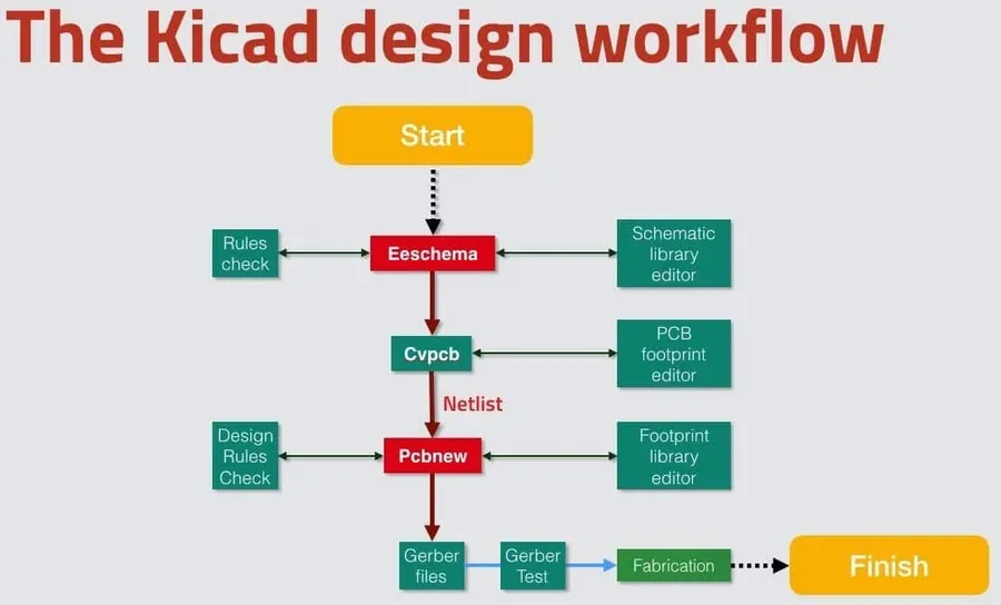
For those seeking powerful PCB design capabilities without incurring costs, several robust, desktop-based software options are available. These open-source tools, such as KiCad and LibrePCB, offer a comprehensive suite of features suitable for both novice and experienced designers. While they may have a steeper initial learning curve compared to some online options, their capacity for complex projects and their flexibility are significant advantages.
| Feature | KiCad | LibrePCB |
|---|---|---|
| Operating System Compatibility | Windows, macOS, Linux | Windows, macOS, Linux |
| Schematic Capture | Advanced, hierarchical support | Modern, user-friendly interface |
| PCB Layout | Feature-rich, 3D visualization | Intuitive, focus on modular design |
| Component Library | Extensive, user-contributed | Growing, standardized library system |
| Simulation | Limited built-in, integration with external tools | Future integration planned |
| Learning Curve | Moderate to steep | Moderate |
| Suitable for | Complex projects, experienced users | Modular designs, users of all levels |
These desktop tools provide a wealth of features without financial investment, making them an ideal choice for designers who require advanced functionality. KiCad is well-suited for complex circuit board designs, while LibrePCB focuses on a modular design workflow. Choosing between these options depends largely on individual preferences and the specific needs of your projects, but both provide a robust, cost-effective solution for PCB design.
Key Features to Look For in a PCB Design Software
Selecting the right PCB design software hinges on identifying essential features that streamline the design process and enhance user experience. An effective tool should facilitate seamless transitions from schematic capture to PCB layout, incorporating robust component management and simulation capabilities, all while ensuring compatibility with industry-standard file formats like Gerber. This enables both novices and experienced designers to efficiently translate their concepts into tangible circuit boards.
| Feature | Description | Importance |
|---|---|---|
| Intuitive Schematic Capture | User-friendly interface for drawing electronic circuits. This typically includes a drag-and-drop interface for components and wiring. | High - Enables quick and accurate circuit design. |
| Comprehensive Component Library | A vast database of components with accurate symbols, footprints, and specifications. Easily manage both standard and custom parts. | High - Speeds up design time and ensures accuracy. |
| Robust PCB Layout Tools | Capabilities for arranging components on a board, creating traces, and managing layers with high levels of precision. | High - Essential for manufacturable and efficient board design. |
| Simulation Capabilities | Tools for simulating circuit performance before physical prototyping. This includes basic voltage and current analysis. | Medium to High - Critical for verifying design integrity and functionality. |
| Gerber File Compatibility | Ability to generate and import standard Gerber files for PCB fabrication. This should also include drill file output and bill of materials output. | High - Necessary for manufacturing process. |
| Design Rule Check (DRC) | Automated checks that identify design errors, such as overlapping traces and insufficient clearances. | High - Prevents manufacturing errors and potential issues. |
| Collaboration Features | Options for multiple users to work on the same project, which is beneficial for team-based designs. | Medium - Streamlines workflows, especially for complex projects. |
Online vs. Offline PCB Design Tools: A Comparison
Selecting the right PCB design tool is crucial for project success, and a key decision revolves around whether to use an online (web-based) or offline (desktop) software solution. Each approach offers distinct advantages and disadvantages, influencing ease of access, collaboration, and the overall design experience. This section provides a comparative analysis to assist in making an informed decision.
| Feature | Online PCB Design Tools | Offline PCB Design Tools |
|---|---|---|
| Accessibility | Accessible from any device with internet; no installation required. | Requires installation on a specific machine; tied to that device. |
| Collaboration | Facilitates real-time collaboration; easy to share projects with others. | Collaboration may require file sharing or version control systems. |
| Updates | Software updates are managed by the provider; always using the latest version. | Requires manual installation of updates and sometimes the risk of incompatibilities. |
| Cost | Often free or subscription-based; may have limitations on advanced features. | Can range from free open-source to expensive commercial licenses. |
| Features | Typically feature rich but may have constraints compared to desktop versions. | Generally more feature-rich, with advanced capabilities for complex designs. |
| Performance | Performance is dependent on internet speed and server stability. | Performance is dependent on local machine resources; generally faster. |
| Stability | Can be more prone to downtime or server issues. | Generally more stable, with less reliance on external resources. |
When deciding between online and offline PCB design tools, consider your individual requirements and workflow. Online tools are excellent for easy access, team projects, and projects where simplicity is preferred. Desktop tools offer more power for demanding projects and professional usage. The choice should align with your project complexity, desired level of collaboration, and available resources.
Step-by-Step Guide to Designing Your First PCB
Designing your first Printed Circuit Board (PCB) can be straightforward when using an 'easy PCB maker' platform. This section provides a practical, step-by-step guide to walk you through the fundamental stages, from creating the schematic to preparing your files for fabrication.
- Define Your Project
Begin by clearly defining the functionality of your PCB. What components do you need, and what is their purpose in the circuit? Simple projects like LED blinkers or basic sensor interfaces are ideal for first-timers. - Choose Your Components
Select the necessary electronic components based on your project requirements. Ensure that you are using the appropriate components with the correct voltage and current ratings from the available component library of your chosen 'easy PCB maker'. Double-check pin assignments, and datasheets as necessary. - Schematic Capture
Using the schematic editor, connect the components according to your circuit design. This stage involves placing symbols representing each component and wiring them to show the electrical connections. Pay close attention to polarity and pin assignments to prevent errors. Refer to component datasheets for accuracy. - PCB Layout
Translate your schematic into a physical board layout. Arrange components within the defined board area, ensuring sufficient spacing and adherence to design constraints. Route traces to connect components according to the schematic. Use your 'easy PCB maker's auto-routing tools, and double check their work. Adjust trace width to handle expected currents. Consider adding thermal pads where needed. - Design Rule Check (DRC)
Perform a DRC to verify your PCB design complies with fabrication specifications. This step identifies issues like incorrect trace spacing or overlaps. Address any detected problems to ensure a manufacturable design. A properly run DRC step will save you time and money in the long run. - Gerber File Generation
Generate Gerber files from your final layout. These are standard files used by PCB manufacturers to fabricate your board. Ensure that all necessary layers are generated, including copper layers, solder mask, and silkscreen. Double check the output against the specifications of your chosen PCB manufacturer. - Fabrication and Assembly
Send your Gerber files to a PCB manufacturing service. Once the boards are produced, assemble the electronic components on the physical PCB by soldering them to the appropriate pads. Test the completed PCB to verify its function and compliance with your initial specifications. Debug and troubleshoot issues, if any.
PCB Design Software for Beginners: Which One is the Easiest?
For beginners venturing into PCB design, selecting the right software is crucial for a smooth learning experience. The ideal software should have an intuitive interface, be easy to navigate, and provide sufficient resources for new users. While professional-grade software offers extensive capabilities, beginner-friendly options focus on simplifying the design process to be more accessible.
Several software options are particularly well-suited for beginners. Fritzing stands out as an excellent choice due to its visually-oriented approach, which allows users to easily transition from breadboard prototypes to PCB designs. Other user-friendly options include Tinkercad Circuits, a browser-based tool known for its simplicity and accessibility. These platforms are designed to minimize the learning curve, enabling new designers to grasp fundamental concepts without getting bogged down by complex functionalities.
| Software | Ease of Use | Learning Curve | Key Features | Best For |
|---|---|---|---|---|
| Fritzing | Very Easy | Low | Visually-oriented interface, breadboard to PCB design | Those transitioning from physical prototypes |
| Tinkercad Circuits | Easy | Low | Browser-based, simple interface | Absolute beginners |
| EasyEDA | Moderate | Medium | Online platform, integrated design environment | Beginners seeking integrated solution |
When selecting a beginner-friendly PCB design software, it is essential to consider your comfort level and familiarity with electronics concepts. Fritzing and Tinkercad are particularly helpful in providing a gentle introduction to PCB design by visualizing physical connections in a way that is easy to understand. As you develop more expertise, exploring more comprehensive platforms such as EasyEDA can enhance your designs. The right starting point depends on the user’s requirements, but simplicity is key to an enjoyable first-time experience.
Frequently Asked Questions about Easy PCB Makers
This section addresses common questions and challenges encountered by new users of easy PCB maker software, focusing on practical solutions to enhance the design and fabrication process. These questions are designed to assist beginners in efficiently utilizing PCB design tools and avoiding common pitfalls.
- How do I select the right electronic components for my PCB design?
Begin by thoroughly understanding your circuit's functional requirements, including voltage, current, and frequency specifications. Consult component datasheets for detailed parameters and verify availability from reliable suppliers. Utilize the component library within your PCB design software. Confirm the footprint matches your required component before placement. - What are Gerber files and why are they needed?
Gerber files are the industry-standard format used to communicate PCB layout information to manufacturers. They contain data on copper layers, solder mask, silkscreen, and drill locations. These files ensure accurate fabrication and assembly by providing the necessary data to a PCB manufacturer's equipment. - How can I generate Gerber files from my PCB design software?
Typically, PCB design software includes a function to generate Gerber files directly from your layout. This process involves selecting the required layers (copper, silkscreen, etc.), setting the appropriate file format, and then exporting the files. Refer to your software's documentation for precise instructions. - Can I integrate my PCB design with fabrication services directly?
Many online and desktop PCB design software platforms offer direct integration with PCB fabrication services, simplifying the ordering process. This usually entails generating Gerber files then uploading them directly through the integrated tool, automatically populating fabrication specifications. Ensure you review the order details and file formats before submitting. - What is the best way to learn how to use an easy PCB maker as a complete beginner?
Start with the software's tutorials, explore the included demo projects, and practice with simple designs. Look for online communities and forums where other users share knowledge. Begin by understanding basic schematic capture and PCB layout, then progress to more advanced functionality. Consistent practice is crucial to mastering any PCB design tool. - How do I choose between online and offline PCB design software for beginners?
Online software offers ease of access and collaboration, typically with simpler interfaces, making them suitable for beginners. Offline software can offer advanced features and control and is typically better for advanced users. If you are a beginner, online software, such as EasyEDA, is likely a better fit. - What are some common mistakes to avoid when using an easy PCB maker?
Common mistakes include incorrect component footprints, inadequate trace widths, insufficient spacing, and improper layer routing. Always double-check your design, use design rule checks within your software, and review component datasheets before committing to fabrication. A design review prior to ordering can prevent errors.
Tips for Optimizing Your PCB Design Process
Optimizing the PCB design process is crucial for reducing errors, improving efficiency, and ultimately creating more reliable and cost-effective circuit boards. This involves careful planning, smart component selection, and strategic use of the capabilities offered by your chosen easy PCB maker.
- Start with a clear schematic:
A well-organized schematic is the foundation of a good PCB layout. Ensure all components are correctly represented and connected before starting on the board layout. It saves significant time in debugging and layout later. - Use component libraries effectively:
Leverage the extensive component libraries available in most PCB design software. Using pre-existing components reduces the likelihood of errors compared to creating components from scratch, which can be time-consuming. Verify every component before use to avoid misrepresentation. - Plan your board layout strategically:
Think about the physical layout early in the process. Place critical components close to their required interaction points. Keep signal paths short and direct to minimize signal integrity issues. Consider heat dissipation requirements and physical constraints. - Utilize auto-routing with caution:
While auto-routers can speed up the layout, it is essential to review the results. Auto-routing algorithms may not always produce optimal routing from a noise or signal integrity perspective, so manual corrections are generally required to fine tune the performance. Manual routing with proper planning can often lead to more efficient and less problematic designs. - Implement Design Rule Checks (DRC) and LVS:
Use DRC to identify any violation of design rules, such as minimum trace width, spacing issues, etc., early in the design phase. Layout Vs Schematic (LVS) ensures the physical layout matches the intended schematic design. Regularly performing DRC and LVS can catch errors that are difficult to detect manually. - Generate accurate Gerber files:
Always double-check the output Gerber files before sending them for fabrication. Review that the drilling data, solder mask, and silkscreen layers are correct. Use a Gerber viewer to ensure that the generated files are as expected and do not have any unwanted overlaps. - Iterate and test:
Plan for iterations; PCB designs may require some tweaks after initial prototype testing. Have your design tested early in the process to identify and rectify errors or performance issues. By testing early and frequently, you increase the reliability of your final design.
The world of PCB design is now more accessible than ever, thanks to the emergence of many easy PCB maker options. By understanding your specific needs, comparing the features of different tools, and following best practices, you can successfully design and fabricate your own custom circuit boards. Whether you are looking for a simple online solution or a comprehensive desktop tool, the right platform is available to bring your electronics vision to reality, especially with the user-friendly options offered by an easy pcb maker. Remember to explore free software options, take advantage of online tutorials, and never stop experimenting to achieve your goals.