Choosing the Right Electronic Board Maker: A Comprehensive Guide
In today's fast-paced tech world, electronic board makers are the unsung heroes behind every gadget and innovation. From simple DIY projects to complex industrial applications, the need for reliable and efficient PCB (Printed Circuit Board) design and fabrication is ever-growing. This article serves as your compass, guiding you through the landscape of electronic board makers, helping you select the best tools and services to bring your electronic visions to life, whether you’re a hobbyist or an industry leader.
Understanding Your PCB Needs
Before selecting an electronic board maker, a meticulous assessment of your project's specific needs is paramount. This initial step dictates the appropriate tools and services, impacting cost, time, and ultimately, the success of your electronic design. A clear definition of design complexity, production volume, time constraints, and budgetary limitations is vital.
The type of board needed significantly influences the selection process. Consider the following:
- Single-layer vs. Multi-layer:
Single-layer boards are simpler and cost-effective for basic designs, while multi-layer boards offer greater design flexibility and increased circuit density for complex projects. - Frequency Requirements:
High-frequency applications require specific materials and design considerations to minimize signal loss and interference, which affects material selection and design parameters. - Complexity and Density:
The complexity of the circuit and the density of components affects the number of layers needed, and influences the necessary software capabilities and fabrication precision. - Component Type:
Whether the design is predominantly surface mount (SMT), through-hole, or a mixture of both, as this will affect the assembly process selection. - Production Volume:
Prototype quantities versus mass production will influence the choice of fabrication and assembly services, affecting turnaround time and cost. - Budget Constraints:
Budget limitations can narrow down the options and may require a compromise between desired features and cost. - Turnaround Time:
The project timeline will determine the choice of fabrication service, as some offer faster turnaround times but at a potentially higher cost.
PCB Design Software: Free vs. Paid Options
The selection of PCB design software is a pivotal decision for any electronics project, directly impacting design complexity, development time, and overall cost. This section navigates the spectrum of available tools, differentiating between free and paid options, and offers insight into their suitability for diverse project scopes.
Free PCB design software provides accessible entry points for hobbyists, students, and smaller projects, and typically offers capable tools for schematic capture and PCB layout. Paid options generally offer advanced capabilities, broader component libraries, and enhanced simulation tools, making them more suited for complex professional projects.
| Feature | Free PCB Design Software | Paid PCB Design Software |
|---|---|---|
| Cost | No direct cost; may have limitations | Requires a license or subscription fee |
| Target User | Hobbyists, beginners, small projects | Professionals, complex projects, larger organizations |
| Component Libraries | May have limited component libraries or community-driven content | Typically includes extensive and regularly updated component libraries |
| Complexity Handling | Suitable for basic to intermediate design complexity | Designed to handle high-complexity and multi-layer PCBs |
| Simulation Capabilities | Often includes basic simulation | Offers advanced simulation and analysis features |
| Technical Support | May have limited technical support, primarily community-based | Includes dedicated technical support and resources |
| Features | Typically includes schematic capture and basic PCB layout tools | Offers advanced features such as signal integrity analysis, 3D visualization, and design rule checks |
| Ease of use | Often have a simpler interface with a lower learning curve | May have a steeper learning curve due to the complexity of the tools |
| Collaboration Features | May have limited collaboration features | Usually offers enhanced team collaboration and version control features |
| Integration with other tools | Integrates with a limited set of external tools | Provides seamless integration with other design and analysis software |
Some free options, such as CircuitMaker and EasyEDA, have user-friendly interfaces and a range of features, making them ideal starting points. Paid software, like Altium Designer, provides a more comprehensive and professional environment with better simulation and collaboration tools, but requires a financial investment. The choice hinges upon project scope and budget.
Key Features to Look for in PCB Design Software
Selecting the appropriate PCB design software hinges on several crucial features that directly impact the efficiency and success of your electronic board design process. These features encompass ease of use, component library richness, simulation capabilities, and flexibility in exporting designs. A careful evaluation of these aspects ensures the software aligns with the user's project scope and requirements, ultimately optimizing the design workflow and ensuring the production of high-quality PCBs.
- Ease of Use
The software should have an intuitive interface with an easily navigable workflow. This reduces the learning curve and minimizes the time spent on administrative tasks, allowing users to focus on the core design activities. Look for features such as clear menus, logical tool placements, and contextual help options. - Comprehensive Component Library
An extensive library of pre-built components is crucial for efficient design. The library should include a broad range of standard and specialized components, along with the ability to easily create custom components. Ensure the library is well-maintained, with up-to-date information and accurate footprints. - Robust Simulation Capabilities
Integrated simulation tools enable the testing of designs for signal integrity, thermal behavior, and electromagnetic compatibility before physical prototyping. The inclusion of both analog and digital simulation features can significantly reduce the potential for costly design flaws and improve overall design quality. - Flexible Export Options
The ability to export designs in standard formats such as Gerber, ODB++, and IPC-2581 ensures that designs can be fabricated by a wide range of manufacturers and used in external tooling. This flexibility promotes interoperability and reduces the potential for incompatibility issues across different fabrication processes. - Integration with Other Design Tools
Assess how well the software integrates with other tools in the engineering workflow. Seamless data exchange between schematic capture, layout, and simulation software enhances efficiency and reduces the potential for errors. The ability to work in a unified environment is particularly beneficial in reducing development time. Compatibility with other programs also ensures a more efficient, well-rounded engineering process. - Collaboration Capabilities
Look for collaboration features, such as version control, real-time sharing, and commenting. These features enable multiple engineers to work on the same project simultaneously. This is particularly important when working in a team environment or with external collaborators, as it promotes consistent and efficient workflows. This reduces potential delays and issues in the project.
Choosing a PCB Fabrication Service
Selecting the right PCB fabrication service is crucial for translating your design into a physical board. These services offer varying capabilities, from prototype runs to large-scale production. The choice depends on factors such as production volume, desired turnaround time, material specifications, and budget. Understanding these factors will enable you to select a manufacturer that meets your project's specific needs.
Several companies specialize in PCB fabrication, offering a range of services tailored to different needs. Companies like JLCPCB and PCBWay are popular choices, particularly for prototyping and small-batch production due to their cost-effectiveness and relatively quick turnaround times. However, it is important to understand the trade offs of cost versus speed versus quality.
| Factor | Description | Considerations |
|---|---|---|
| Turnaround Time | The time it takes from submitting your design to receiving the fabricated boards. | Express services may be available for faster turnaround, but typically at a higher cost. |
| Material Selection | The type of substrate material used for the PCB, such as FR-4, aluminum, or flexible substrates. | Different materials have different electrical and mechanical properties, affecting performance and durability. Consider the operating environment of the board. |
| Cost | The total expense for PCB fabrication, including any additional charges for specific features or services. | Compare quotes from different manufacturers and understand the cost breakdown for each. |
| Manufacturing Capabilities | The range of technological options, such as minimum trace width, layer count, via type and drill size | Match the service's capabilities to the complexity of your PCB design. Some designs have greater needs in terms of feature sizing. |
| Quality Control | The processes in place to ensure the manufactured PCBs meet the required specifications. | Check for certifications such as ISO 9001, and request inspection reports. |
Certifications play a pivotal role in assessing the quality and reliability of a PCB fabrication service. Manufacturers with certifications like ISO 9001 demonstrate a commitment to quality management. These certifications often reflect rigorous processes and testing, ensuring that the PCBs meet industry standards. Requesting inspection reports and understanding the company's quality control procedures will also help to determine the reliability of their service.
Understanding PCB Assembly Services
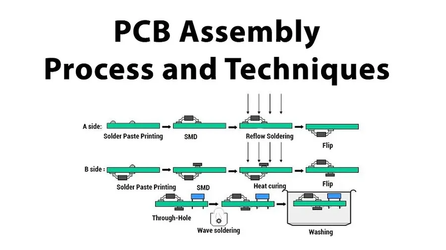
PCB assembly services are crucial for transforming bare printed circuit boards into functional electronic devices. These services encompass the precise placement and soldering of electronic components onto the PCB, streamlining the manufacturing process and saving considerable time and resources for designers and manufacturers alike. The choice of assembly method depends on the project's complexity, scale, and component types.
- Surface Mount Technology (SMT)
SMT involves mounting components directly onto the surface of the PCB, which is ideal for high-density designs and automated assembly. SMT components are typically smaller and lighter than through-hole components. - Through-Hole Technology (THT)
THT involves inserting component leads through pre-drilled holes on the PCB and soldering them on the opposite side. This method is suitable for larger components that require greater mechanical strength and is often used for prototypes or for components where surface mounting is not feasible. - Mixed Assembly
Mixed assembly combines SMT and THT, accommodating projects that require both surface mount and through-hole components for optimal functionality and performance. This approach allows for design flexibility and caters to a wide range of component types.
The selection of components for PCB assembly also plays a vital role. Components are categorized based on their mounting technology (SMT, THT), type (resistors, capacitors, ICs), and physical size. For automated assembly, pick-and-place machines require components packaged on reels or trays. Furthermore, design for manufacturability (DFM) and design for assembly (DFA) are best practices to minimize assembly costs and reduce errors during the assembly process.
| Factor | Description |
|---|---|
| Assembly Type | SMT, THT, or Mixed Assembly based on component types and requirements |
| Component Types | Selection of components based on technology, physical size, and function. |
| Volume of production | Cost-effectiveness of automation for large-scale production. Manual assembly can be cheaper for low-volume. |
| Level of Automation | Pick and place automation reduces cost and improves quality in large-scale production. |
Rapid Prototyping with Desktop PCB Printers
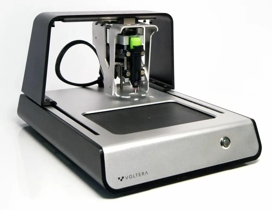
Desktop PCB printers offer a compelling alternative for rapid prototyping, allowing engineers to create circuit boards in-house, significantly reducing turnaround times compared to traditional fabrication services. These devices are particularly useful for iterative design processes, enabling real-time feedback and adjustments.
The core advantage of desktop PCB printers lies in their ability to quickly produce prototypes, enabling engineers to test and iterate on designs rapidly without relying on external fabrication services. This real-time feedback loop is invaluable for accelerating the design process and quickly uncovering design flaws.
| Feature | Desktop PCB Printers | Third-Party Fabricators |
|---|---|---|
| Turnaround Time | Hours | Days/Weeks |
| Cost per Prototype | Potentially Lower (long term) but High initial investment | Variable, depends on complexity and quantity |
| Design Iteration | Very Fast and In-House | Slower, relies on fabrication queue |
| Complexity | Limited to simpler designs, often single or double-layer boards | Can handle complex, multi-layer boards |
| Precision | Lower | Higher |
| Materials | Limited to specific materials (ink) | Wider selection available |
| Initial Investment | Higher | Lower |
A notable example of a desktop PCB printer is the Voltera V-One, which integrates printing, reflow, and dispensing functionalities. These features enable a more streamlined prototyping process. Despite the appeal of these devices, it is essential to consider their limitations. They may not be suitable for complex multi-layer boards or large production runs. The precision and material choices may also be more constrained compared to professional fabrication houses.
The financial aspect of desktop PCB printers is also something to consider. While the per-prototype cost may be lower in the long term, the upfront investment in the machine can be substantial. Therefore, the cost-effectiveness hinges on the frequency of prototyping and the type of projects undertaken. Engineers should carefully evaluate their specific needs and compare these to the capabilities of desktop printers before making an investment decision.
Frequently Asked Questions About Electronic Board Makers
This section addresses common queries regarding electronic board makers, covering the board creation process, cost considerations, manufacturing equipment, and recommendations for manufacturers and software. Understanding these aspects is crucial for anyone involved in PCB design and fabrication.
- What is the typical process of making an electronic board?
The process generally begins with designing the circuit using PCB design software, which involves creating a schematic and then laying out the board. Next, the design is exported in a format suitable for manufacturing. The board is then fabricated by a PCB manufacturer, which may include etching, drilling, and plating processes. Finally, the electronic components are assembled onto the board, typically through soldering. - How much does it cost to make an electronic board?
The cost of making an electronic board can vary widely depending on several factors. These include the complexity of the design (single-layer vs. multi-layer), the size of the board, the quantity needed (prototype vs. mass production), the materials used, and the choice of fabrication and assembly services. Basic prototype boards can cost tens of dollars, while complex, mass-produced boards can run into thousands or more. Software costs vary greatly too, and a detailed cost analysis of your specific needs is vital. - What type of machinery is used in circuit board manufacturing?
Circuit board manufacturing utilizes a variety of specialized machinery. This includes equipment for precision drilling, chemical etching for creating conductive traces, plating equipment for adding layers of metal, and pick-and-place machines for automated component assembly. In addition, solder reflow ovens and inspection equipment like AOI machines (Automated Optical Inspection) ensure the quality of the final product. The level of machinery sophistication is highly dependent on the complexity and volume required. - Which manufacturers are known for producing quality electronic boards?
Several manufacturers are recognized for their quality and service. JLCPCB and PCBWay are popular for their prototype and small-batch production services. For higher volume production, companies such as TTM Technologies and Sanmina are well regarded. The choice of manufacturer often depends on the project requirements, desired quality, cost constraints, and production volume. Always obtain quotes from multiple vendors, and choose based on the overall project needs. - What are some recommended software options for designing electronic boards?
There are numerous software options available for PCB design, catering to various levels of complexity and user experience. Free options like EasyEDA and KiCad are excellent for beginners and hobbyists. For more advanced and professional use, paid software such as Altium Designer and Cadence OrCAD offer a wider range of features and capabilities. Choosing the right software depends on the complexity of your project, your budget, and your familiarity with PCB design tools. - Can I make a PCB at home?
Yes, it is possible to create PCBs at home, but the process is usually limited to simpler, single or double-layer boards. Methods include using a laser printer for toner transfer, etching with chemicals, and manual drilling. Desktop PCB printers, like the Voltera V-One, provide more advanced capabilities for in-house prototyping. However, for complex or multi-layered boards, it is generally more reliable and cost-effective to use a professional fabrication service due to higher quality and reliability. - What is the role of simulation in PCB design?
Simulation plays a critical role in modern PCB design by allowing engineers to test the performance of their designs before physical fabrication. Simulation software can analyze signal integrity, thermal behavior, and electromagnetic compatibility issues, preventing costly errors and enabling engineers to fine-tune their circuits and layout. It's an essential step to mitigate risks, especially for high-frequency and complex designs, ultimately saving time and resources.
Comparative Analysis of PCB Board Makers
Selecting the right electronic board maker is crucial for project success. This section offers a comparative analysis of popular options, focusing on their core strengths, pricing models, and target audiences. This structured comparison aids users in making informed decisions aligned with their specific needs and project goals.
| Board Maker | Core Strengths | Pricing | Target Audience | Key Features | Limitations |
|---|---|---|---|---|---|
| EasyEDA | User-friendly interface, free tier available, integrated online design and fabrication. | Free for basic use; paid options for advanced features and increased fabrication quantities. | Hobbyists, beginners, and small-scale projects. | Schematic capture, PCB layout, integrated fabrication service, large component library. | Limited advanced simulation capabilities. |
| CircuitMaker | Free professional-grade software, active online community, powerful design tools. | Free for personal and commercial use. | Professionals, advanced users, and larger projects. | Advanced routing, simulation, and collaboration features, extensive component library. | Steeper learning curve for beginners. |
| Altium Designer | Industry-leading software with advanced features for complex designs, powerful simulation capabilities. | Subscription-based, higher cost, considered an industry standard | Professional engineers, large-scale projects, complex designs. | High-speed design, advanced simulation and analysis, team collaboration, extensive component library. | High cost, requires powerful hardware and more complex to learn. |
| JLCPCB | Affordable PCB fabrication and assembly, quick turnaround, a wide range of manufacturing capabilities. | Competitive pricing, various discounts available. | Professionals, hobbyists, and medium to large scale projects | PCB fabrication, assembly services, parts sourcing and multiple layer options. | Can be limited to certain size constraints. |
| PCBWay | Full-service PCB fabrication and assembly, supports advanced technologies. | Competitive pricing with variable options for prototypes and bulk production. | Professionals, larger scale projects, high-complexity boards | High precision PCB fabrication, assembly, parts sourcing, testing services and rigid-flex PCBs. | Turnaround time and complex orders require more planning |
| Voltera V-One | Desktop PCB printer for rapid prototyping, real-time feedback on design | Higher initial cost, but may save time and resources. | Engineers who need rapid testing, real-time feedback, small-batch production. | Rapid prototyping on the desktop, instant feedback on your design, custom substrates and dual layer printing. | Limited to smaller boards, not suitable for mass production. |
The world of electronic board makers is vast and varied. By understanding your project's requirements, exploring the diverse options for PCB design software and fabrication services, and keeping an eye on emerging technologies like desktop PCB printers, you can make informed decisions that lead to successful and innovative electronic designs. Remember to choose an electronic board maker that aligns with your budget, timeline, and technical capabilities to maximize your success in electronics design, whether you are a hobbyist or part of a large scale organization. The goal is to empower you with the right knowledge to navigate this complex field.