Choosing the Right High Frequency PCB Manufacturer: A Comprehensive Guide
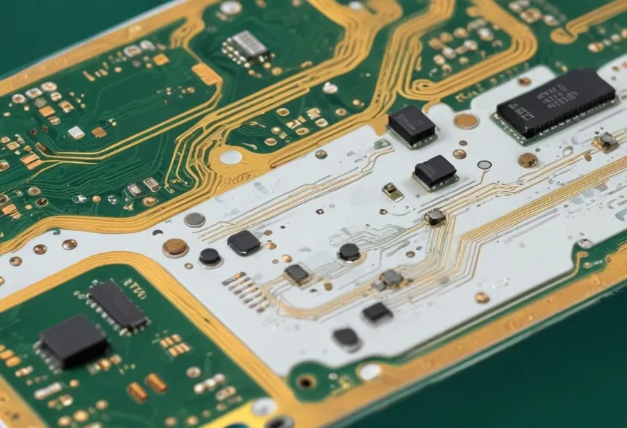
In today's fast-paced technological landscape, high frequency printed circuit boards (PCBs) are the backbone of countless devices, from smartphones to advanced radar systems. These specialized PCBs, often fabricated by a high frequency pcb manufacturer, demand precision and expertise to ensure signal integrity and optimal performance. This article explores the key factors to consider when selecting a high frequency PCB manufacturer and offers guidance to ensure your project's success.
Understanding High Frequency PCBs
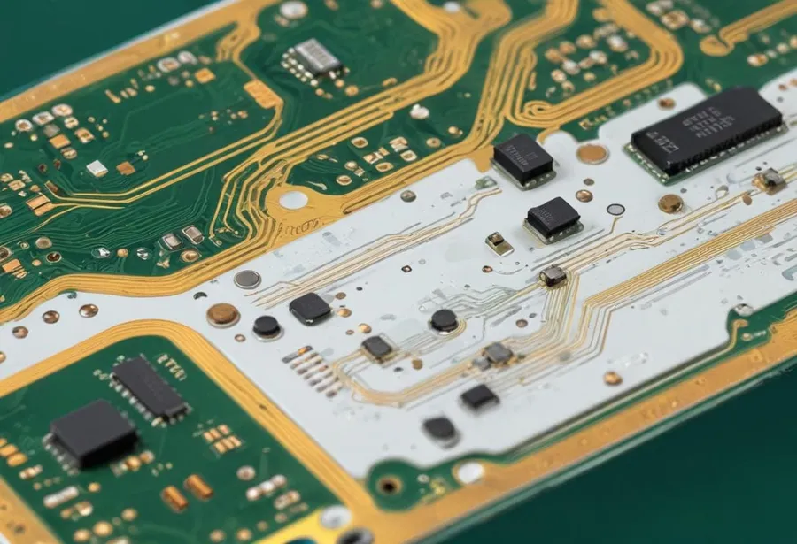
High-frequency PCBs are specialized circuit boards designed to operate effectively at elevated frequencies, typically exceeding 1 GHz. These PCBs are crucial for applications where signal integrity and minimal signal loss are paramount. Unlike standard PCBs, they require materials and designs that can manage the unique challenges posed by high-frequency signals, such as impedance control, reduced signal reflections, and minimal dielectric losses.
The fundamental differences between high-frequency, radio frequency (RF), and standard PCBs are significant. Standard PCBs, often made from FR-4 material, are adequate for lower-frequency digital and analog applications. RF PCBs, while also operating at high frequencies, are specifically designed for radio frequency signal transmission, often requiring specialized impedance matching and shielding. High-frequency PCBs represent a broader category, encompassing boards designed to operate in elevated frequency ranges that may not be specifically RF but require controlled impedance and low signal loss characteristics. The challenges in manufacturing high-frequency PCBs involve achieving very tight tolerances in the PCB's physical characteristics and the material properties of its dielectric. Material selection is critical, as the dielectric constant and loss tangent of the material directly impact signal quality at high frequencies. Moreover, specialized processes are required to fabricate these PCBs accurately.
Key Materials for High Frequency PCBs
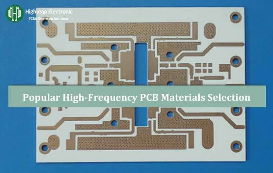
The selection of appropriate materials is paramount in the fabrication of high-frequency PCBs, as these materials significantly influence the electrical performance, thermal management, and overall reliability of the final product. This section details the common materials used, emphasizing their properties and applications.
| Material | Dielectric Constant (εr) | Loss Tangent (tan δ) | Thermal Conductivity (W/m·K) | Typical Applications | Cost |
|---|---|---|---|---|---|
| Rogers RO4000 Series | 3.38 - 3.66 | 0.002 - 0.003 | 0.6 - 0.7 | Aerospace, Automotive Radar, Wireless Communications | Moderate to High |
| PTFE (Teflon) | 2.1 - 2.6 | 0.0001 - 0.0004 | 0.25 | High-end RF applications, Microwave circuits | High |
| FR-4 (with High-Tg) | 4.2-4.8 | 0.018-0.025 | 0.3-0.4 | General High-frequency applications,Cost-sensitive designs | Low to moderate |
| Ceramic-filled laminates | 2.5 - 10 | 0.001- 0.005 | 1-4 | High-power RF amplifiers, High-temperature environments | High |
| Hydrocarbon-based laminates | 2.8-3.5 | 0.002-0.004 | 0.3 - 0.4 | Automotive radar, Antennas | Moderate |
The table above offers a comparative overview. Rogers RO4000 series provides a good balance of performance and cost and is often selected for applications with demanding yet not extreme needs. PTFE (Teflon) offers exceptional electrical performance, particularly its low loss tangent, making it suitable for high-end RF and microwave applications. FR-4, especially high-Tg variations, can be used in less demanding high-frequency applications where cost is a primary consideration. Ceramic-filled laminates are used when thermal management and high operating temperatures are critical. Hydrocarbon-based laminates bridge a gap with good performance and moderate costs for automotive and antenna applications.
- Dielectric Constant (εr)
This represents a material's ability to store electrical energy. For high-frequency applications, a stable and low dielectric constant is important to ensure consistent signal transmission speed and minimize signal reflections. Changes in εr can cause impedance mismatches leading to signal degradation. - Loss Tangent (tan δ)
The loss tangent indicates how much energy is dissipated as heat within the material at high frequencies. A low loss tangent is crucial to reduce signal attenuation and maintain signal integrity, particularly over long traces. High loss tangents result in energy wastage and heat generation. - Thermal Conductivity
This refers to how efficiently a material transfers heat. High thermal conductivity is essential to manage heat generated by high-speed circuits and high power components and to prevent material degradation due to thermal stresses and to maintain the operational performance of the PCBs. - Material Suitability
Material suitability depends on the operating frequency range, the application’s environmental conditions (temperature, humidity), and required reliability, including mechanical properties. Different PCB materials offer specific advantages and trade-offs that need to be considered.
Critical Design Considerations for High Frequency PCBs
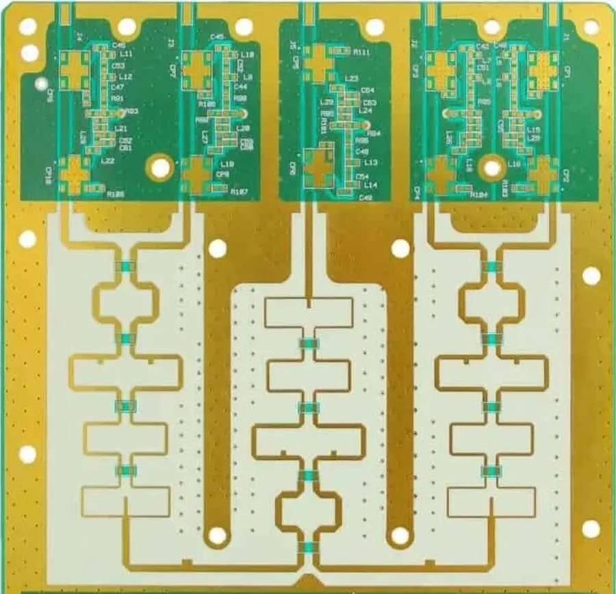
High-frequency PCB design requires meticulous attention to detail to maintain signal integrity and minimize losses. This section outlines crucial design considerations for high-frequency PCB layouts, focusing on impedance control, trace routing, ground planes, and via design, all critical for minimizing signal loss and reflections.
- Impedance Control
Precise impedance matching is paramount in high-frequency circuits to minimize signal reflections and ensure efficient power transfer. Controlled impedance traces are achieved by carefully managing trace width, spacing, and dielectric properties. This is typically implemented using a microstrip or stripline configuration. - Trace Routing
Trace routing in high-frequency PCBs demands careful planning to avoid sharp bends, which can cause signal reflections and impedance discontinuities. Optimal routing involves the use of smooth curves and minimal trace lengths. Additionally, differential pairs require matched lengths and close proximity to minimize skew and maintain common-mode noise rejection. - Ground Planes
Solid ground planes are essential for high-frequency PCB designs. They provide a low-impedance return path for signals, reduce noise, and facilitate controlled impedance. Ground planes must be continuous and free of breaks or gaps, and connected to all ground points in the circuit. Multiple layers with ground planes may be required. - Via Design
Vias, essential for layer transitions, can introduce impedance discontinuities and signal reflections at high frequencies. Minimize via count where possible and use plated-through vias with smaller diameters and annular rings for optimal performance. Via stitching is also used to connect multiple ground vias, creating low inductance paths - Minimizing Signal Loss and Reflections
Achieving minimal signal loss and reflections requires careful management of several factors. Dielectric materials with low loss tangents, smooth trace geometries, precise impedance control, and robust ground plane design are critical. Using appropriate stack-ups and low-loss connectors contribute to reduced losses. Signal reflections can also be reduced by effective termination techniques.
Evaluating High Frequency PCB Manufacturers
Selecting the right high-frequency PCB manufacturer is paramount to ensuring the performance and reliability of your high-speed electronic products. This section outlines the critical criteria to consider when evaluating potential manufacturers, focusing on their capabilities, experience, certifications, and quality assurance processes.
- Experience and Expertise
A manufacturer with a proven track record in producing high-frequency PCBs is essential. Look for experience with various high-frequency materials (e.g., Rogers, PTFE) and a deep understanding of the design challenges associated with these types of PCBs. - Certifications and Compliance
Verify that the manufacturer holds relevant certifications such as ISO 9001 (quality management), ISO 14001 (environmental management), UL (product safety), and RoHS (Restriction of Hazardous Substances). These certifications demonstrate a commitment to quality and environmental responsibility. - Production Capabilities
Assess the manufacturer's production capacity, including their ability to handle your required board sizes, layer counts, and volume. Ensure that their equipment is suitable for high-frequency PCB manufacturing, including precision etching, controlled impedance capabilities, and laser drilling. - Material Expertise
The manufacturer should have in-depth knowledge of high-frequency materials. They should be able to advise on material selection based on your application's frequency, thermal, and environmental requirements. They should have good vendor relationships to ensure high quality materials are used. - Quality Control Processes
Rigorous quality control is critical for high-frequency PCBs. Inquire about the manufacturer's testing procedures, including impedance testing, signal integrity testing, and dielectric constant measurement. Look for a manufacturer with robust inspection protocols at every stage of production. - Testing and Verification
Beyond standard PCB testing, verify that the manufacturer offers specific testing for high-frequency applications such as Time-Domain Reflectometry (TDR) and Network Analysis, to ensure that the impedance control and signal performance meet the required design parameters - Lead Times
Evaluate lead times for both prototype and production runs. A manufacturer with flexible and transparent production schedules is crucial to meet your project deadlines.
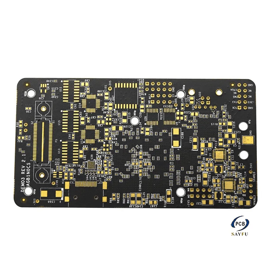
High Frequency PCB Manufacturing Processes
The fabrication of high frequency PCBs demands meticulous control and precision throughout each stage of the process, from initial material selection to final surface finish. These processes are crucial for ensuring the board's performance, signal integrity, and reliability in high-frequency applications. Given the sensitivity of high-frequency signals, even minor deviations in manufacturing can significantly impact the performance of the circuit. Therefore, maintaining tight tolerances and stringent quality control measures are paramount.
- Material Selection
The process begins with the selection of appropriate high-frequency materials. These materials, such as Rogers RO4000 series or PTFE (Teflon), are chosen based on their specific electrical properties like dielectric constant (Dk) and loss tangent (tan δ), which are crucial for high-frequency signal transmission. This stage includes rigorous inspection for material defects. - Cutting and Preparation
Once selected, the raw material is precisely cut to the required dimensions, and prepared with the necessary treatment for subsequent processing. This might involve cleaning and applying a photoresist layer. - Imaging and Patterning
Using photolithography, the circuit pattern is transferred onto the PCB material. The material coated with photoresist is exposed to UV light through a mask containing the circuit pattern. This process creates a hardened image of the circuit, allowing for the selective removal of the photoresist. - Etching
The exposed copper is then removed using a chemical etching process, leaving behind the desired circuit traces. The etching process requires precise control to maintain the specified trace widths and spacing, which are critical for high-frequency performance. - Layer Alignment and Lamination
For multilayer boards, this is a critical step. Inner layers are aligned precisely and then laminated together using a combination of heat and pressure. This process must ensure the layers bond securely without air gaps or misalignment. - Drilling
Holes for vias and component mounting are drilled using precision drilling machines. The drilling process must be accurate to avoid damaging the circuit. The size and location of these holes are critical for signal integrity and component placement. - Plating
The drilled holes are plated to create conductive pathways for interlayer connections, i.e. vias. This is typically done with copper. The plating process must provide a uniform and reliable conductive layer. - Solder Mask Application
A solder mask is applied to the PCB to protect it from environmental factors and to prevent solder bridging during assembly. Precise alignment and even application of the solder mask are essential. - Surface Finishing
The final step before assembly is surface finishing, which is applied to ensure good solderability and prevent oxidation. Common finishes include HASL (Hot Air Solder Leveling), ENIG (Electroless Nickel Immersion Gold), and others. The chosen finish must be compatible with the intended use and environment. - Testing and Quality Control
The completed PCB undergoes rigorous testing procedures, including electrical testing, impedance testing, and visual inspection. This ensures each board meets the required performance specifications and quality standards before it is passed on for assembly.
Frequently Asked Questions about High Frequency PCBs
This section addresses common queries regarding high-frequency PCBs, providing concise and authoritative answers to assist in understanding their unique characteristics, applications, and manufacturing considerations.
- What frequency range is considered high frequency for PCBs?
There isn't a universally defined threshold, but generally, PCBs operating above 1 GHz are considered high frequency. Frequencies in the multi-GHz range are increasingly common, especially with the advent of advanced wireless technologies and faster digital data transfer rates. The specific classification also depends on the application and the materials used, as certain materials may exhibit high frequency behavior at lower values due to material loss or impedance changes. - How do high frequency PCBs impact signal integrity?
High frequency PCBs significantly impact signal integrity due to several factors. At higher frequencies, signal wavelengths become shorter, leading to increased signal reflections and losses if impedance is not carefully controlled. Dielectric losses in materials become more pronounced, causing signal attenuation. Proper design, such as impedance matching, controlled trace routing, and the use of appropriate materials, are critical to maintaining signal integrity in high-frequency applications. Any discontinuities in the signal path, such as vias or bends, also have a more significant impact as frequencies increase. - What are the main challenges in manufacturing high frequency PCBs?
Manufacturing high frequency PCBs presents unique challenges. Maintaining tight impedance tolerances, managing material characteristics such as dielectric constant and loss tangent, and ensuring precision in trace geometries are crucial. The materials are often more expensive and require specialized handling, and the manufacturing process has to be very precise and controlled. Special drilling and plating are often required to achieve the necessary quality. High frequency PCB manufacturing also needs specific expertise, high-precision equipment, and meticulous quality control. - What are the cost implications of using high frequency materials?
High frequency materials often have a higher cost than standard PCB materials like FR-4 due to their specialized properties and manufacturing processes. Materials such as Rogers laminates or PTFE have better signal integrity performance but are more costly and require more care in fabrication. The need for precise fabrication, coupled with potential material waste due to tight tolerances, further contributes to the cost, which can be significantly higher than using lower-grade materials. - How does material selection affect the performance of high frequency PCBs?
Material selection is paramount for performance in high frequency PCBs. The dielectric constant (Dk) and loss tangent (Df) of the material determine signal velocity and losses, respectively. Lower Df materials are preferred to minimize signal attenuation at higher frequencies. The thermal stability and expansion coefficients also affect long term performance and board reliability in varying environmental conditions. Selecting the right material ensures optimal signal transmission, minimal signal loss and maintains consistent electrical characteristics. - Are there any special handling requirements for high frequency PCB materials?
Yes, high frequency PCB materials often require special handling due to their unique properties. Many of these materials are sensitive to moisture absorption, requiring careful storage in controlled humidity environments. Some laminates, especially PTFE-based materials, need precise etching parameters and processing temperatures. Proper personal protective equipment (PPE) and training are needed for personnel during manufacturing, as these materials can present hazards if not handled correctly. Special cleaning methods may also be needed to prevent contamination and ensure the best possible performance of the manufactured PCB. - What is the impact of trace routing on signal integrity in High Frequency PCBs?
Trace routing is a major factor in high frequency PCB design. In High frequency PCBs, even small changes in trace impedance may lead to signal reflections and loss which degrade performance. Impedance control ensures the energy is efficiently transmitted, minimizing signal reflections and maintaining clarity. High frequency signals are also sensitive to discontinuities so sharp angles in routing should be avoided as they can result in reflections. Length matching is also essential in differential pair routing to ensure signals arrive at their destination in phase with each other. Proper grounding also eliminates unwanted signal noise. Careful planning and execution of trace routing are crucial for optimum performance in high frequency PCBs.
Cost Factors in High Frequency PCB Manufacturing
The cost of manufacturing high frequency PCBs is a multifaceted consideration influenced by several interconnected factors. Understanding these cost drivers is crucial for optimizing design choices and ensuring cost-effective production, especially given the specialized materials and processes involved.
Material selection is a primary cost driver. High-performance laminates such as Rogers RO4000 series and PTFE (Teflon) are significantly more expensive than standard FR-4 materials, primarily due to their superior electrical properties like lower dielectric loss and consistent dielectric constant over a wide frequency range. These materials are essential for high-frequency applications but contribute directly to increased costs. The cost also increases with material thickness and the surface finish requirements. The overall cost is further affected by fabrication requirements, board complexity and lead times.
PCB complexity, particularly the number of layers, is a significant cost factor. Multilayer PCBs require more complex fabrication processes, involving multiple lamination steps, via drilling, and plating, which drives up production costs. Complex board shapes, dense component layouts, and the use of specialized features such as blind and buried vias also increase fabrication time and cost.
Production volume has a direct impact on the cost per unit. Prototype runs, with their lower volumes, incur higher setup costs and per-unit prices due to the overhead of setting up the manufacturing process. Mass production, on the other hand, benefits from economies of scale, leading to lower per-unit costs as fixed costs are spread across a larger number of boards. Therefore, the decision between prototype and mass production will substantially affect overall cost. Optimizing material utilization is a vital aspect of cost reduction when considering high volume production.
Lead time is another critical cost consideration. Expedited manufacturing, often required for tight project deadlines, can result in higher costs due to the prioritization of production and potential overtime charges. Balancing lead times with project timelines is vital to optimize cost and delivery schedules. Lead time can be affected by the chosen fabrication process and the availability of the high frequency materials, requiring advanced planning. Efficient material procurement and optimized board designs can assist with both lead times and the overall cost. Selecting a PCB manufacturer with optimized lead times for the chosen materials is essential.
| Cost Factor | Impact on Cost | Optimization Strategies |
|---|---|---|
| Material Choice | High-performance materials (e.g., Rogers) significantly increase cost. | Use lower-cost materials where performance requirements allow, optimize material usage by selecting optimum panel sizes for production. |
| Layer Count | More layers increase fabrication complexity and cost. | Minimize layer count by optimizing design, where possible, whilst maintaining required performance parameters. |
| Board Complexity | Complex shapes, dense component layouts and special vias drive up costs. | Simplify design where possible, consider design rule checks that optimise both performance and cost. |
| Production Volume | Prototype runs are more expensive per unit than mass production. | Consolidate orders, plan production volumes effectively to maximize economy of scale. |
| Lead Time | Expedited manufacturing increases cost. | Plan for realistic lead times and design schedules, communicate effectively with your manufacturer. |
Future Trends in High Frequency PCB Technology
The high-frequency PCB landscape is rapidly evolving, driven by demands for higher data rates, smaller device footprints, and more robust performance in increasingly challenging environments. These trends are pushing the boundaries of materials science, manufacturing processes, and design techniques, paving the way for innovative solutions across diverse industries.
- Advanced Materials
Emerging materials with lower dielectric constants, lower loss tangents, and improved thermal conductivity are being developed to enable higher frequency operation and greater signal integrity. These include novel polymers, ceramics, and composites that offer enhanced performance characteristics. - Miniaturization and Integration
There is a strong trend towards smaller, more densely packed PCBs to reduce device size and increase functionality. Advanced manufacturing techniques such as microvia technology and fine-line etching are crucial for achieving these goals. This also involves integration of passive components into the PCB substrate, further reducing overall size. - Increased Integration with Other Technologies
High-frequency PCBs are becoming increasingly integrated with other technologies like advanced packaging methods (e.g., system-in-package), and novel interconnect solutions (e.g., 3D interconnects). This integration facilitates complex functionalities and performance enhancements. - 5G and Beyond
The relentless expansion of 5G networks is pushing the boundaries of high-frequency PCB design and manufacturing. Future telecommunications technologies will demand even more sophisticated PCB solutions that can operate at millimeter wave frequencies. The automotive industry is seeing a rise in applications such as radar for driver assistance systems and automotive communication where reliability in extreme conditions is important. - Aerospace Advancements
The aerospace sector requires high-frequency PCBs that can operate reliably in extreme temperature ranges, withstand mechanical vibrations, and meet stringent weight constraints. Future trends include advanced lightweight materials and designs to meet the demands of complex avionics and satellite systems.
Comparative Analysis: High Frequency PCB Materials
Selecting the appropriate material is paramount in high-frequency PCB design, as it directly impacts signal integrity, performance, and cost. This section provides a comparative analysis of common high-frequency PCB materials, focusing on their key electrical and thermal properties.
| Material | Dielectric Constant (Dk) | Loss Tangent (Tan δ) | Thermal Conductivity (W/m·K) | Cost | Typical Applications |
|---|---|---|---|---|---|
| Rogers RO4350B | 3.48 | 0.0037 | 0.65 | Medium | Wireless infrastructure, aerospace, automotive radar |
| Rogers RO4003C | 3.55 | 0.0027 | 0.8 | Medium-High | High-speed digital, microwave circuits, RF applications |
| Rogers RO3003 | 3.0 | 0.0013 | 0.39 | High | Millimeter-wave applications, radar, satellite communications |
| PTFE (Teflon) | 2.1-2.6 | 0.0002-0.0005 | 0.25 | High | Aerospace, microwave, high-reliability applications |
| FR-4 (Standard) | 4.2-4.8 | 0.02 | 0.3 | Low | General-purpose PCBs, low-frequency applications (Not suitable for high-frequency) |
| Nelco N4000-13EP | 3.66 | 0.009 | 0.35 | Medium | High Speed Digital, communication infrastructure |
| Isola I-Tera MT40 | 3.45 | 0.0032 | 0.54 | Medium-High | Automotive radar, advanced driver assistance systems(ADAS) |
Key considerations when choosing a material include the operating frequency, signal integrity requirements, thermal management needs, and cost constraints. Materials like Rogers RO4000 series offer a good balance of performance and cost for many high-frequency applications, while PTFE based materials are chosen when lowest possible signal losses are critical. FR-4, though inexpensive is not suitable for high frequency applications due to high dielectric loss and inconsistent properties at higher frequencies. Selecting a material is not just about properties, but also about reliability and processability. Manufacturers need to be familiar with the material’s characteristics. Always consult with your chosen PCB manufacturer for material availability and cost implications.
Choosing the right high frequency PCB manufacturer is crucial for the success of any high-frequency electronic project. By carefully considering the materials, design challenges, and manufacturing processes, and selecting a manufacturer with expertise in high frequency technologies, you can ensure the production of reliable and high-performing PCBs. As technology continues to advance, the importance of high frequency PCBs will only increase, making it imperative to stay informed and choose a high frequency pcb manufacturer that can meet your evolving needs.