Choosing the Right Multi Layer PCB Manufacturer: A Comprehensive Guide
In today's technologically advanced world, multi-layer PCBs form the backbone of countless electronic devices, from smartphones to sophisticated medical equipment. Selecting a reliable multi layer PCB manufacturer is crucial for ensuring the success of any project. This article will delve into the essential factors to consider when choosing a manufacturer and will guide you through the complexities of multilayer PCB fabrication, helping you make an informed decision for a successful outcome.
Understanding Multilayer PCB Basics
Multilayer PCBs are circuit boards comprised of three or more conductive layers of copper, separated by insulating material, enabling greater circuit density and complexity than single or double-sided boards. Their increased capability makes them essential in sophisticated electronic devices across industries.
- Advantages over Single/Double-Sided PCBs
Multilayer PCBs offer higher circuit density, reduced board size, improved signal integrity, and enhanced functionality compared to their single or double-sided counterparts. - Common Applications
These advanced boards are widely utilized in applications requiring high performance and miniaturization, including but not limited to computer motherboards, smartphones, aerospace systems, and medical equipment.
Key Factors in Selecting a Multi Layer PCB Manufacturer
Selecting the right multi layer PCB manufacturer is crucial for ensuring the quality, reliability, and performance of your electronic products. This decision hinges on several key factors that directly impact the final product, including manufacturing capabilities, material options, certifications, lead times, and pricing. A thorough evaluation of these aspects is essential to find a manufacturer that aligns with your project's technical and budgetary requirements.
| Factor | Description | Importance |
|---|---|---|
| Fabrication Capabilities | Number of layers, minimum trace width/spacing, blind/buried vias, aspect ratio for drilling | Ensures the manufacturer can produce your design's specific requirements and complexity. |
| Material Options | Availability of various materials like FR-4, Rogers, and high-frequency laminates | Matches the material properties to the electrical and thermal requirements of the application. |
| Certifications | ISO 9001, ISO 13485, UL certifications | Indicates the manufacturer's adherence to quality standards and compliance. |
| Lead Times | Turnaround time for PCB fabrication | Ensures timely delivery to meet production schedules. |
| Pricing | Cost per board, tooling costs, additional fees | Fits the project within budget while considering quality and complexity. |
Layer Count and Complexity in Multilayer PCBs
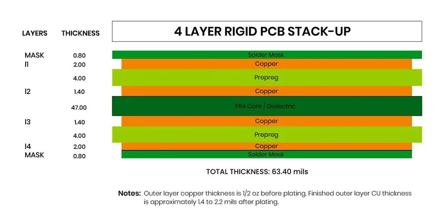
The layer count in a multilayer PCB directly influences its functionality, performance, and cost. Ranging from simple 4-layer boards to highly complex designs with 32, 60, or more layers, the number of layers dictates the routing capacity, signal integrity, and overall complexity of the circuit board. Increased layers allow for more intricate circuit designs, more power and ground planes, and reduced signal crosstalk.
| Layer Count | Complexity | Typical Applications | Cost Implications |
|---|---|---|---|
| 4-Layer | Relatively simple | Basic consumer electronics, simple industrial controls | Lower cost |
| 6-Layer | Moderate complexity | Advanced consumer electronics, some industrial applications | Moderate cost |
| 8-12 Layer | Increased complexity | Networking equipment, high-speed computing, medical devices | Higher cost |
| 14-20 Layer | High complexity | Advanced networking hardware, complex telecommunications equipment | Higher cost |
| 20+ Layer | Very high complexity | High-performance servers, advanced aerospace applications | Very high cost |
The choice of layer count is not arbitrary; it's a balance between performance requirements and cost constraints. Higher layer counts, while offering more routing space and better signal integrity, also increase manufacturing costs due to the complexity of fabrication. Therefore, a careful evaluation of the design's needs and budgetary limitations is required during the design phase.
Furthermore, layer count directly affects the PCB's stack-up. A well-defined stack-up is critical for impedance control and signal integrity, especially in high-speed applications. The arrangement and spacing of the layers, including power and ground planes, contribute significantly to the overall electrical performance of the PCB.
Material Selection for Multilayer PCBs
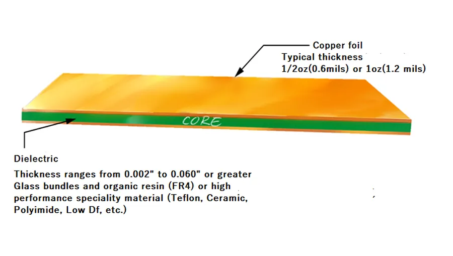
The selection of materials for multilayer PCBs is paramount to achieving desired performance characteristics, moving beyond the standard FR-4 to encompass a range of specialized laminates. These materials cater to diverse applications, each with its unique set of thermal, electrical, and mechanical properties impacting signal integrity and operational reliability.
| Material | Dielectric Constant (εr) | Dissipation Factor (tan δ) | Thermal Conductivity (W/m·K) | Typical Applications |
|---|---|---|---|---|
| FR-4 | 4.0-4.8 | 0.02 | 0.2-0.3 | General purpose, low-cost applications |
| High Tg FR-4 | 4.2-4.6 | 0.015-0.02 | 0.25-0.35 | Higher temperature applications, improved reliability |
| Rogers 4350B | 3.66 | 0.0037 | 0.67 | High frequency, impedance control, RF applications |
| Rogers 4003C | 3.55 | 0.0027 | 0.69 | High speed digital, broadband applications |
| Isola I-Speed | 3.68 | 0.0045 | 0.28 | High speed digital, low loss applications |
| Polyimide | 3.2-3.5 | 0.002-0.004 | 0.3 | Flexible PCBs, high-temperature environments |
Beyond the commonly used FR-4, materials such as Rogers laminates are employed in high-frequency applications due to their low dielectric constant and dissipation factor, crucial for signal integrity at higher frequencies. Polyimide substrates are selected for flexible PCBs and applications demanding thermal stability. When choosing materials, thermal properties like the coefficient of thermal expansion (CTE) and thermal conductivity must be considered, along with impedance control and mechanical durability.
Multilayer PCB Fabrication Processes
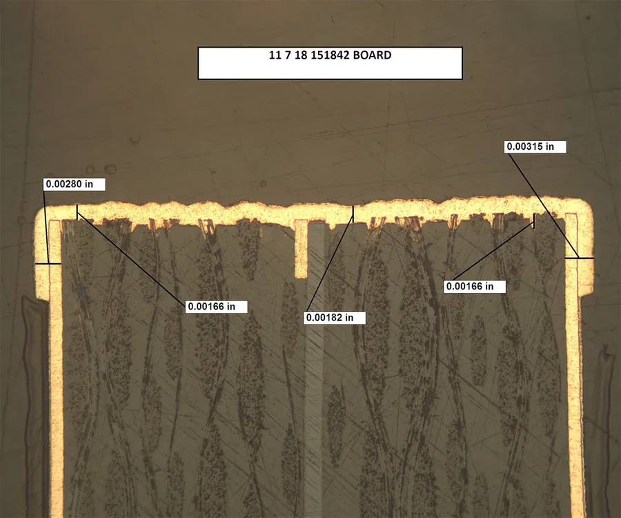
The fabrication of multilayer PCBs is a complex process involving several stages, each crucial for ensuring the final product's reliability and performance. These stages include lamination, drilling, plating, and quality assurance, with special attention given to via formation techniques like blind, buried, and through vias. Understanding these processes is essential for both manufacturers and designers to optimize the fabrication and design of multi layer PCB.
Below is a breakdown of the key stages involved:
- Inner Layer Processing
This stage involves creating the individual circuit layers, usually through photolithography and etching. Each layer is made from copper-clad laminate and is patterned using UV-sensitive film, where the unwanted copper is removed chemically. - Lamination
The individual inner layers are stacked together with prepreg (a semi-cured epoxy resin) between them. This stack is then pressed under high temperature and pressure in a process known as lamination. This fuses the layers together, forming the multilayer board. - Drilling
After lamination, holes are drilled to create vias. These vias provide electrical connections between different layers. The drilling process requires high precision and is performed using automated machinery with computer-controlled settings. - Plating
The drilled holes and the surface of the PCB are then chemically plated with copper, making the vias conductive. This is followed by pattern plating to add conductive copper to the outer layers of the board. - Etching of Outer Layers
Similar to inner layer processing, the outer layers are patterned using photolithography and etching to create the final circuit traces and pads. Unwanted copper is removed, leaving the circuit design. - Solder Mask Application
A solder mask, usually a green epoxy ink, is applied to the PCB surface to protect the circuits from oxidation and to prevent solder bridges during assembly. The solder mask is applied through screen printing or photolithography. - Surface Finish
The final step is applying a surface finish to improve solderability and corrosion resistance. Common surface finishes include HASL (Hot Air Solder Leveling), ENIG (Electroless Nickel Immersion Gold), and immersion tin or silver. - Quality Control and Testing
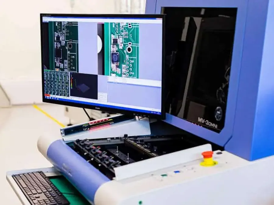
Throughout the fabrication process and after completion, quality control checks and electrical tests are performed to ensure the boards meet the design specifications and are free of defects. These may include visual inspections, AOI (Automated Optical Inspection), and electrical tests, like flying probe or in-circuit testing.
Via Formation Techniques:
- Through Vias
These are the simplest type of vias, extending through all layers of the board. They are the easiest to manufacture but can limit routing space on inner layers. - Blind Vias
These vias connect an outer layer to one or more inner layers, but do not go through the entire board. They provide more routing flexibility than through vias. - Buried Vias
These vias connect only internal layers and are not visible on the outer surfaces of the board. They are even more complex to fabricate than blind vias but offer the highest routing density.
Frequently Asked Questions about Multi Layer PCB Manufacturing
This section addresses common queries regarding multi-layer PCB manufacturing, providing clarity on the nuances of design, fabrication, and cost considerations to empower informed decision-making.
- Can a PCB have an odd number of layers, such as three layers?
While technically possible, three-layer PCBs are uncommon due to the manufacturing challenges and the increased cost. Standard PCB fabrication processes usually involve pairing layers for symmetrical stack-ups, which are more stable and less prone to warping. Therefore, most multi-layer boards begin with four layers, as they are more practical and cost-effective. - What are the criteria for selecting the best PCB manufacturer?
The 'best' PCB manufacturer varies based on project needs, however, key factors include fabrication capabilities (layer count, via types, tolerances), material options, certifications (ISO, UL), lead times, pricing, and customer support. A thorough review of their past work, testimonials, and communication is essential for a successful partnership. It's also vital to check if they can meet specific project requirements such as impedance control, high-frequency requirements, or HDI manufacturing techniques. - How exactly are multi-layer PCBs manufactured?
Multi-layer PCB manufacturing involves a sequence of precise steps: Firstly, individual layers are etched on thin copper sheets bonded to dielectric material. These layers are then carefully stacked and laminated under high heat and pressure, bonding them together. Holes are drilled using precise CNC machines for vias, which connect different layers. Finally, the board undergoes plating to create conductive paths, and surface finishing is applied. This complex process requires sophisticated machinery and rigorous quality control. - Who are the largest and most reputable PCB suppliers globally?
Identifying the 'largest' PCB supplier can vary depending on the data source and scope of measurement. However, some of the leading manufacturers are often recognized for their large-scale production and sophisticated capabilities. These companies often have large global operations and are known for serving diverse industries including electronics, automotive and aerospace. Public financial data from market analysis reports and industry publications can provide insight into the leading companies. - What is the fundamental difference between a 2-layer PCB and a multi-layer PCB?
A 2-layer PCB has conductive copper layers on its top and bottom surfaces only, limiting routing complexity and functionality. Multi-layer PCBs, conversely, feature three or more conductive layers within the board, separated by insulating material. This allows for higher circuit density, improved signal integrity, and enables more complex designs. - How does material selection impact the cost of multi-layer PCBs?
The material used has a substantial impact on cost. FR-4 is the most common and affordable choice. However, high-performance materials such as Rogers laminates, which offer better electrical and thermal characteristics, are more expensive and are often used in higher-frequency applications. High-speed materials may need advanced processing, increasing the cost further, and cost of multi layer pcb is affected directly by the number of layers needed, but more significantly by the materials used, special features, and tolerances required. - What are some best design practices for multi-layer PCBs?
Effective multi-layer PCB design requires meticulous planning, focusing on signal integrity, thermal management, and manufacturability. Key practices include proper layer stack-up design to reduce crosstalk, impedance matching to ensure signal quality, sufficient power and ground planes, strategic via placement for efficient routing, and adherence to manufacturer design rules to avoid problems in production.
Quality Control and Certifications for Multi Layer PCB Manufacturing
Rigorous quality control and adherence to international standards are paramount in multilayer PCB manufacturing. These measures not only ensure the reliability and performance of the PCBs but also reflect the manufacturer's commitment to delivering high-quality products.
Evaluating a multi layer PCB manufacturer involves a thorough examination of their quality control processes and certifications. A robust quality system minimizes defects, optimizes yields, and ultimately reduces the total cost and risk associated with PCB production.
- ISO 9001 Certification
ISO 9001 certification demonstrates a manufacturer's commitment to a robust Quality Management System (QMS). It ensures consistent processes, from design review to final inspection, resulting in high-quality PCBs. - IPC Standards Adherence
Adherence to IPC standards (e.g., IPC-A-600, IPC-6012) is crucial for PCB manufacturing, covering aspects from design guidelines to acceptance criteria. Compliance with these standards demonstrates the manufacturer's capabilities and commitment to quality. - UL Certification
Underwriters Laboratories (UL) certification indicates that the PCB product or process meets specific safety requirements and standards. UL certification is crucial for product safety and regulatory compliance. - Testing Protocols
Quality assurance is maintained through various testing methods during manufacturing, including Automated Optical Inspection (AOI), Flying Probe testing and Electrical Testing. This approach ensures the detection and rectification of potential issues early in the process. - Material Traceability
A reliable manufacturer should have a robust system for tracing materials used in the PCB. This provides assurance about the quality and suitability of materials used.
Cost Optimization Strategies for Multilayer PCBs
Optimizing the cost of multilayer PCBs requires a multifaceted approach, encompassing design choices, material selection, and strategic procurement practices. By focusing on these key areas, significant reductions in overall manufacturing expenses can be achieved without compromising performance or reliability. This section delves into actionable strategies for cost-effective multilayer PCB production.
- Design Optimization
Efficient layout and routing can minimize the board area and material usage. Reducing the number of layers or optimizing via placement can also decrease manufacturing complexity and, consequently, cost. Consider using fewer blind and buried vias where possible, as these add to the cost and production time. Simplifying the design can significantly reduce the fabrication cost. - Material Selection
While high-performance materials offer superior characteristics, standard materials like FR-4 are often sufficient for many applications and are more cost-effective. Evaluate the necessary material properties against the cost. If thermal performance isn't a primary concern, opting for the standard material can considerably lower production expenses. Consider using lower cost alternative materials, where performance is not heavily impacted. - Volume Ordering
Manufacturing costs per unit often decrease as the production volume increases. When planning a project, anticipating future needs can lead to cost savings. Establishing a good relationship with a reliable manufacturer and ordering in bulk is a more economical approach for recurring projects or high-demand products. - Panelization
Panelizing designs (arranging multiple PCBs on a single manufacturing panel) can optimize the usage of material and reduce per-unit fabrication cost. Proper panelization can save money and is a common practice that should be discussed with your manufacturer early on. - Standardized Designs
Utilizing standardized components and layouts can streamline the manufacturing process and reduce setup costs. By using the same footprint or common circuit blocks you will gain from economies of scale from the manufacturer. - Negotiating with the Manufacturer
Engage with your manufacturer early in the design process. They can provide valuable insights on design for manufacturability and suggest cost-saving alternatives. Establishing a relationship and being transparent with manufacturing goals will aid in negotiating price, and lead times.
Future Trends in Multi Layer PCB Technology
The multi layer PCB industry is in constant evolution, driven by demands for higher performance, smaller form factors, and enhanced functionality. Emerging trends are shaping the future of PCB technology, impacting both design and manufacturing processes. These advancements aim to overcome the limitations of current technologies, pushing the boundaries of what's achievable in electronic devices.
- Advanced Substrates
Beyond traditional FR-4, there's a push towards using materials with superior electrical, thermal, and mechanical properties. These include high-performance laminates, ceramics, and flexible substrates that enable more complex and reliable designs, especially in high-frequency applications. - Miniaturization Techniques
Driven by the demand for smaller and more integrated electronic devices, techniques like microvias, high-density interconnects (HDI), and fine-line etching are gaining importance. These allow for higher component density and improved electrical performance in a smaller area. - 3D Printing and Additive Manufacturing
Additive manufacturing methods, including 3D printing, are transforming PCB fabrication. These technologies can potentially reduce prototyping lead times and enable more complex three-dimensional circuit structures. While still relatively new, they hold the potential to revolutionize the industry in the future. - Embedded Components
Integrating passive components directly into the PCB substrate reduces board space, increases component density, and improves overall circuit performance. This is especially important for high-frequency circuits and for applications requiring compact designs. - Advanced Thermal Management
As electronic devices become more powerful, effective thermal management is crucial. Future PCBs will likely feature improved heat dissipation technologies, such as embedded heat spreaders, and materials with higher thermal conductivity. - Sustainable and Eco-Friendly Materials
Growing environmental awareness is prompting a shift towards using sustainable and eco-friendly materials for PCB fabrication. This involves using materials with lower environmental impact, improved recyclability, and greener manufacturing processes.
Selecting the right multi layer PCB manufacturer is paramount for the successful realization of electronic products. By considering factors like technical capabilities, material options, quality certifications, and pricing, you can choose a manufacturer who fits the needs of your product and ensure that you are set up for success. The evolving landscape of technology brings new opportunities and challenges, staying informed and working with a reliable multi layer PCB manufacturer is essential for future advancements.