Choosing the Right RF PCB Manufacturer: A Comprehensive Guide
In our increasingly wireless world, RF PCBs are the unsung heroes behind countless applications, from satellite communications to advanced radar systems. Selecting the right RF PCB manufacturer is critical to ensure the reliability and performance of these systems. This article delves into the key factors to consider when choosing an RF PCB manufacturer, examining what sets leading manufacturers apart and how to approach the selection process to meet your specific needs, ensuring that [rf pcb manufacturer] plays a crucial role in the success of your high-frequency designs.
Understanding RF PCB Requirements
Radio Frequency (RF) PCBs operate at high frequencies, demanding stringent design and manufacturing processes to maintain signal integrity and optimal performance. These unique requirements, including high-frequency signal management, precise impedance control, and minimal signal loss, necessitate specialized expertise from RF PCB manufacturers. Understanding these demands is the first crucial step in selecting a suitable manufacturing partner.
- High-Frequency Performance
RF PCBs operate in the MHz to GHz range, requiring materials and designs that can handle these frequencies with minimal signal degradation. This includes considerations for dielectric constant and loss tangent of the substrate material. - Impedance Control
Maintaining a consistent impedance throughout the signal path is critical to prevent signal reflections and ensure efficient power transfer. This requires precise control over trace widths, spacing, and dielectric properties of the board material. - Signal Integrity
Signal integrity refers to the quality of the electrical signal as it travels through the PCB. Factors such as reflections, crosstalk, and electromagnetic interference (EMI) need to be carefully managed during design and manufacturing. - Material Selection
The choice of substrate materials plays a crucial role in determining the electrical performance of an RF PCB. Materials like PTFE and Rogers, known for their low dielectric loss and stable electrical properties at high frequencies, are often preferred over standard FR4 material for critical RF applications. - Manufacturing Precision
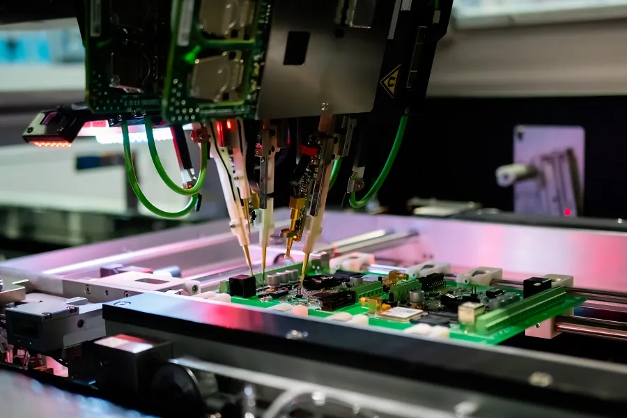
RF PCB manufacturing demands higher precision than standard PCBs to achieve the tight tolerances required for high-frequency applications. This involves careful control of trace etching, layer alignment, and via drilling.
Key Capabilities of an RF PCB Manufacturer
Selecting an RF PCB manufacturer requires careful consideration of their core competencies, which are crucial for ensuring the performance and reliability of the final product. These capabilities extend beyond standard PCB fabrication and necessitate specialized expertise in high-frequency design, materials, and testing.
- Material Expertise
A manufacturer should demonstrate extensive knowledge and experience with RF-specific materials such as PTFE (Teflon), Rogers, and other high-frequency laminates. This includes understanding their dielectric properties, thermal stability, and how these characteristics impact high-frequency signal performance. They should be able to advise on material selection based on the specific application requirements. - High-Layer Count Capability
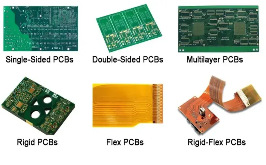
Modern RF applications often require complex, multi-layered PCBs to achieve the necessary circuit density and signal routing. An experienced RF PCB manufacturer should possess the ability to produce boards with a high layer count, maintaining precise alignment and impedance control across all layers. - Advanced Testing Facilities
Comprehensive testing is critical for RF PCBs. The manufacturer should possess advanced testing equipment, including vector network analyzers (VNAs), time-domain reflectometers (TDRs), and signal integrity analysis tools. These tools are vital for verifying impedance matching, signal loss, and overall performance of the fabricated boards. They should also adhere to stringent testing standards. - Precise Impedance Control
Maintaining precise impedance control is crucial for signal integrity in RF circuits. The manufacturer must demonstrate the ability to control trace widths, spacing, and dielectric properties accurately to ensure that the PCB meets specified impedance targets, minimizing signal reflections and losses. - Microvia and Fine-Line Technology
RF designs frequently require microvias and fine-line traces to achieve compact layouts and high-density interconnections. A competent manufacturer should have the technology and expertise to produce these fine features consistently while maintaining signal integrity and reliability. - DFM (Design for Manufacturability) Expertise
An RF PCB manufacturer should not only fabricate PCBs according to design specifications but also offer DFM expertise. This includes providing feedback on design choices that could impact manufacturability, performance, and cost.
Material Selection for RF PCBs
The selection of substrate materials is paramount in the design and manufacturing of Radio Frequency (RF) PCBs. These materials directly influence the high-frequency performance, signal integrity, and overall reliability of the RF circuit. An experienced RF PCB manufacturer plays a crucial role in guiding these material choices, providing expertise that aligns with specific application requirements.
Different materials offer varying dielectric constants, loss tangents, and thermal properties, which affect impedance control, signal attenuation, and the operating temperature range of the PCB. The manufacturer's expertise in handling and processing these materials is just as important as the properties of the materials themselves. Common materials include, but are not limited to, FR-4, PTFE (Teflon), and ceramics, each suited for distinct applications based on their performance characteristics. The choice significantly impacts manufacturability, cost, and the final performance of the RF PCB.
| Material | Dielectric Constant (εr) | Loss Tangent (tan δ) | Typical Applications | Cost | Advantages | Disadvantages |
|---|---|---|---|---|---|---|
| FR-4 | 4.3 - 4.7 | 0.020 | General RF applications, low frequency applications | Low | Cost-effective, widely available, good mechanical properties | High loss at higher frequencies, less precise impedance control |
| PTFE (Teflon) | 2.1 - 3.5 | 0.0001 - 0.002 | High frequency, Low loss applications | High | Low loss, excellent for high frequency, good stability | More expensive, difficult to process, prone to deformation |
| Ceramics | 6-10 | 0.001-0.004 | High frequency, high power applications | Very High | High thermal conductivity, high temperature stability, excellent mechanical strength | Very expensive, difficult to process and large PCB size is difficult to process |
Design for Manufacturability (DFM) in RF PCBs
Design for Manufacturability (DFM) in RF PCBs is a critical process that ensures the design specifications are not only functional but also readily achievable within the manufacturing capabilities of the selected RF PCB manufacturer. It involves a collaborative effort between the designer and the manufacturer, focusing on optimizing the PCB layout for performance while adhering to manufacturing constraints. This process directly impacts the board's overall reliability and performance, particularly at high frequencies where even minor deviations can result in significant signal degradation.
DFM for RF PCBs involves careful consideration of several key aspects:
- Impedance Control
Maintaining consistent impedance throughout the signal path is crucial for RF circuits to avoid signal reflections and losses. DFM ensures that trace widths, spacing, and dielectric properties are designed to achieve target impedance values, typically 50 ohms. Manufacturers use controlled impedance processes to fabricate the boards with the required precision. - Trace Design and Routing
RF traces are often designed as transmission lines. DFM considerations include minimizing bends and discontinuities in traces to avoid impedance changes, ensuring proper spacing to reduce crosstalk between adjacent signals, and managing trace lengths to ensure accurate signal timing and avoid resonance at critical frequencies. The manufacturer’s capabilities with precise etching and trace definition become vital. - Via Placement
Vias introduce parasitic inductance and capacitance, which can negatively affect signal integrity at high frequencies. DFM focuses on minimizing the number of vias, using optimized via sizes and types, and strategically placing them to minimize their impact on signal performance. The manufacturer's capacity to create high-precision vias is crucial. - Material Selection Impact
DFM also considers the material properties selected, like dielectric constant and loss tangent, and how these interact with design choices for signal transmission efficiency. Working with manufacturers that have deep experience with specialized RF materials is crucial for successful designs.
The collaboration between the RF PCB designer and manufacturer during the DFM process is key. Early involvement of the manufacturer in the design phase allows for necessary adjustments to be made proactively, mitigating potential manufacturing issues that could lead to poor performance or delays. This collaborative approach leverages the manufacturer’s expertise to ensure that the PCB design not only meets performance requirements but is also optimized for efficient and reliable production.
Quality Control and Testing for RF PCBs
Rigorous quality control and testing are paramount in RF PCB manufacturing to ensure that the final product meets stringent performance requirements. A reputable RF PCB manufacturer employs a suite of testing procedures to verify the integrity of the board, crucial for applications where signal fidelity and reliability are non-negotiable. These tests cover various parameters including impedance control, signal loss, and structural integrity, often guided by established certifications.
- Impedance Testing
Ensures that the characteristic impedance of traces and transmission lines matches design specifications. This is crucial for preventing signal reflections and maintaining signal integrity. - Signal Loss Measurement
Measures signal attenuation across the board at different frequencies. It verifies that the board performs to design requirements in terms of signal transmission efficiency, a key factor in high-frequency applications. - Time-Domain Reflectometry (TDR)
Used to analyze signal reflections and impedance variations along traces. It can identify discontinuities and anomalies in the signal path. - Network Analysis
Characterizes the frequency response of the PCB, providing insights into transmission parameters and reflection coefficients across the frequency range of operation. - Functional Testing
Validates the performance of the PCB in a simulated or actual operating environment. It includes tests for functionality, power consumption, and signal integrity. - Visual Inspection
A detailed visual examination of the PCB, verifying that the materials, solder joints, and components conform to the quality standards and specifications. Checks for defects, such as opens, shorts, or any kind of visible damage. - Environmental Testing
Evaluating a PCB’s performance under different temperature and humidity levels to ensure reliability in varying conditions.
Certifications like ISO 9001, AS9100 and IATF 16949 further validate a manufacturer's commitment to quality. ISO 9001 is a general quality management system standard, while AS9100 is tailored for the aerospace industry, and IATF 16949 is designed for automotive industry, all indicating adherence to specific quality management system requirements. Manufacturers holding these certifications demonstrates that they have processes in place to ensure repeatable, reliable production and testing of RF PCBs.
Cost Considerations for RF PCB Manufacturing
Understanding the cost drivers in RF PCB manufacturing is crucial for making informed decisions. Balancing cost with performance and quality requires careful consideration of various factors, from material selection to the complexity of the design, and ultimately the choice of your RF PCB manufacturer. These decisions impact both the initial expenditure and the long-term reliability and performance of the final product.
| Cost Factor | Description | Impact on Overall Cost |
|---|---|---|
| Material Costs | The type of substrate material (e.g., FR4, PTFE, Rogers) significantly impacts cost. High-performance materials like PTFE are generally more expensive. | High |
| Layer Count and Complexity | Higher layer counts and intricate designs increase manufacturing complexity, leading to higher costs. | Medium to High |
| Lead Time | Shorter lead times or expedited production often incur higher manufacturing costs, especially for quick-turn prototyping. | Medium |
| Manufacturing Processes | Specialized processes like precision etching, laser drilling, and controlled impedance techniques all contribute to cost. | Medium |
| Testing and Quality Control | Rigorous testing procedures, including signal integrity and impedance testing, will raise the production costs. However, investing in comprehensive testing ensures higher reliability. | Medium |
| Order Volume | Large production runs often result in lower per-unit costs due to economies of scale. | Low to High |
| Manufacturer Location | Geographic location of manufacturer will impact shipping costs, import duties, and potentially labor rates, which will affect total costs. | Low to Medium |
Frequently Asked Questions About RF PCB Manufacturing
This section addresses common questions regarding RF PCB manufacturing, offering insights into typical lead times, crucial design aspects, and the capabilities of high-frequency flexible PCBs. Understanding these aspects is crucial for making informed decisions when selecting an RF PCB manufacturer.
- What are typical lead times for RF PCB orders?
Lead times for RF PCBs can vary significantly depending on complexity, material availability, and the manufacturer's current workload. Standard lead times can range from a few days for simple prototypes to several weeks for complex, high-layer count boards. Expedited services are often available at a premium. - What are the most critical aspects of RF PCB design to ensure impedance matching?
Impedance matching is vital in RF circuits to minimize signal reflections and ensure efficient power transfer. Key design aspects include precise trace width and spacing, controlled dielectric materials, and proper use of ground planes. Simulation tools and design rule checks are essential for verification. - Can high-frequency PCBs also be flexible?
Yes, high-frequency PCBs can be made flexible using materials like flexible substrates such as polyimide or PTFE. These materials have low dielectric loss and offer the required electrical performance for high-frequency operation. However, they can be more expensive and require specialized manufacturing techniques. - What materials are commonly used for RF PCBs?
Common materials include FR4 for less demanding applications, while higher-performance applications use materials like Rogers, PTFE (Teflon), and ceramics. These materials offer superior dielectric constants, lower losses, and thermal stability, crucial for high-frequency circuits. The choice is based on a cost versus performance trade-off. - How does the layer count of an RF PCB affect its performance and cost?
Higher layer counts allow for more complex circuit designs, better signal routing, and increased signal integrity by dedicating layers to ground planes. However, increasing the layer count also increases manufacturing cost, complexity, and lead time. There is a point of diminishing return, where increased layers do not add any benefit. - What testing procedures are crucial for RF PCBs to ensure quality?
Critical tests include impedance testing (TDR), insertion loss testing, and return loss testing using a network analyser. Visual inspection for defects and solder joint integrity are also required for quality assurance. Reliability testing, including thermal cycling and vibration tests, are used to further test the PCB. - How does the choice of surface finish affect RF performance?
Surface finishes impact solderability and signal conductivity. Common finishes include ENIG (Electroless Nickel Immersion Gold) which provides good solderability and minimal oxidation. HASL (Hot Air Solder Leveling) is cost-effective but may not be ideal for high-frequency due to variable thickness. The selection of surface finish must be done with an understanding of electrical and mechanical requirements.
Comparing Different RF PCB Manufacturers
Selecting the right RF PCB manufacturer requires a thorough comparison of their capabilities and offerings. A practical comparison table allows for an objective evaluation based on critical factors such as material expertise, lead times, pricing, and the availability of advanced services. This structured approach ensures that the final choice aligns with the specific requirements of your RF PCB application.
| Attribute | Manufacturer A | Manufacturer B | Manufacturer C | Manufacturer D |
|---|---|---|---|---|
| Material Expertise | Extensive (PTFE, Rogers, Ceramics) | Good (PTFE, FR4) | Limited (FR4, Standard Rogers) | Moderate (PTFE, FR4) |
| High Layer Count | Up to 24 layers | Up to 16 layers | Up to 12 layers | Up to 18 layers |
| Lead Times (Standard) | 2-3 weeks | 3-4 weeks | 4-6 weeks | 2-4 weeks |
| Lead Times (Expedited) | 1-2 weeks | 2 weeks | Not Available | 1 week |
| Price (Relative) | High | Moderate | Low | Moderate-High |
| Advanced Services | Impedance control, microvias, blind/buried vias | Impedance control, blind vias | Basic Impedance control | Impedance control, microvias |
| Testing Facilities | Full suite, including signal integrity analysis | Standard testing, basic signal integrity | Basic Electrical Testing | Full suite, signal integrity analysis |
| Certifications | ISO 9001, AS9100 | ISO 9001 | ISO 9001 | ISO 9001, AS9100 |
Future Trends in RF PCB Manufacturing
The field of RF PCB manufacturing is dynamic, undergoing continuous evolution driven by the demands for higher performance, smaller form factors, and more versatile applications. Staying informed about these trends is crucial for selecting an RF PCB manufacturer that can meet current and future needs.
- Miniaturization
The demand for smaller, more compact electronic devices is pushing the limits of PCB manufacturing. Advanced techniques such as microvias, high-density interconnect (HDI) technology, and finer line widths and spacing are becoming more prevalent. A forward-thinking manufacturer will invest in these capabilities. - Advanced Materials
Traditional materials like FR4 may not always meet the requirements of next-generation RF applications. There is an increasing use of materials with superior electrical properties, such as low-loss laminates, advanced ceramics, and even flexible substrates. Manufacturers need to demonstrate expertise in handling these materials. - Integration of Components
Integrating passive components directly into the PCB substrate, as well as components like antenna-in-package (AiP), reduces the need for discrete devices and allows for more compact and efficient RF designs. The RF PCB manufacturer needs to be experienced in these integration techniques. - 3D Printing and Additive Manufacturing
Additive manufacturing technologies are showing promise for the fabrication of RF PCBs with complex geometries and custom features, opening up the potential for faster prototyping and greater design freedom, a manufacturer embracing these processes will likely be able to meet future needs better. - Sustainability
As environmental concerns grow, there's a move towards more sustainable practices in PCB manufacturing, including the use of eco-friendly materials and waste reduction strategies. Choosing a manufacturer that's dedicated to sustainable practices can align with long term goals.
Choosing the right RF PCB manufacturer is essential for realizing high-performance RF and microwave applications. By focusing on capabilities, materials, quality, and cost factors, this article equips you with the information to ensure the success of your project. A reliable [rf pcb manufacturer] should be a partner in design innovation. Remember, the right partner will ensure that your PCB design is manufactured with precision, leading to high-performance results and reliability. They will adapt to future trends, ensuring their product continues to meet industry standards.