Decoding PCB Fabrication Costs: A Comprehensive Guide for 2024
Printed circuit boards (PCBs) are the unsung heroes of modern electronics, quietly enabling everything from smartphones to satellites. But before your brilliant design comes to life, you need to navigate the world of PCB fabrication costs. Just as the price of a custom-tailored suit differs from a ready-made one, PCB fabrication costs can vary widely based on a multitude of factors. This article cuts through the noise, providing a clear and comprehensive guide on what drives these costs and how you can optimize your project without sacrificing quality.
Key Factors Influencing PCB Fabrication Costs
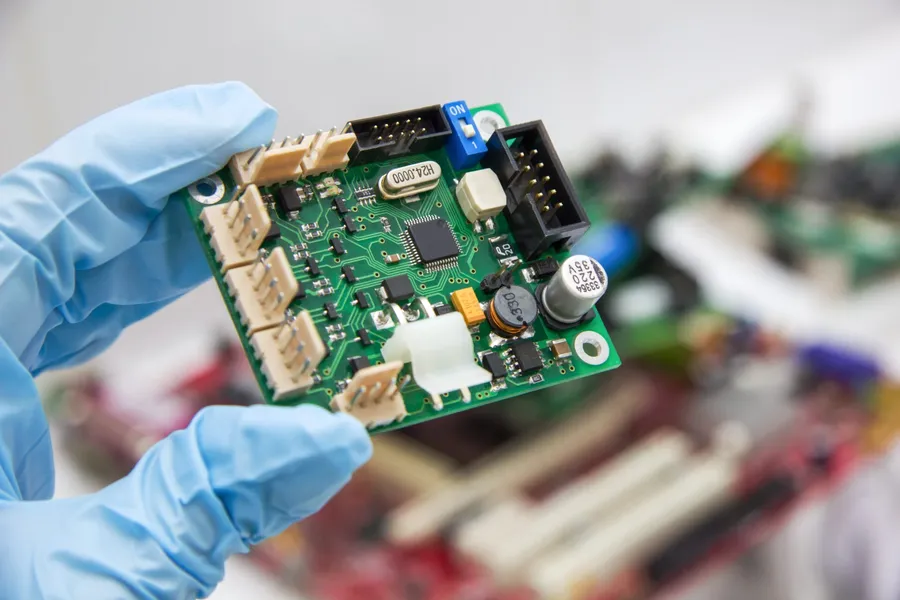
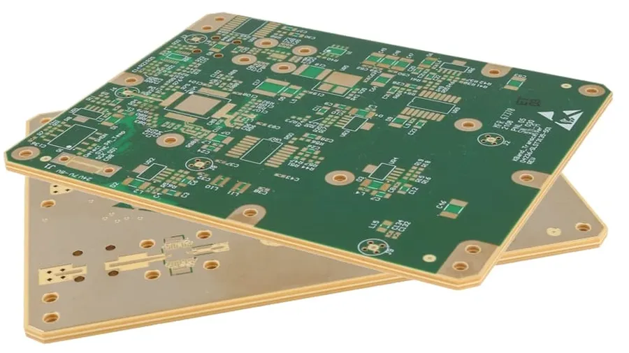
Understanding the primary cost drivers in PCB fabrication is crucial for managing expenses effectively. Several key factors significantly influence the final price of a printed circuit board, including the board's dimensions, the number of conductive layers, the materials chosen, and the overall design complexity. Each of these aspects directly contributes to the manufacturing effort and resource consumption, thereby impacting the total cost.
| Factor | Description | Impact on Cost |
|---|---|---|
| Board Size | The physical dimensions of the PCB. | Larger boards require more material and processing time, increasing costs. |
| Layer Count | The number of conductive layers in the PCB. | More layers mean more complex manufacturing processes and higher costs. |
| Material Selection | The type of substrate used (e.g., FR-4, Aluminum, Rogers). | Different materials have varying costs and processing requirements, impacting overall price. |
| Design Complexity | The density of components, trace width, vias, and the overall intricacy of the circuit design. | More complex designs require more precise manufacturing and increase costs |
Material Matters: Impact on PCB Price
The selection of PCB material is a critical factor influencing both the performance and cost of the final product. Different materials offer varying electrical, thermal, and mechanical properties, leading to diverse cost implications. This section explores the most common PCB materials and their respective cost trade-offs.
| Material | Description | Cost | Typical Applications | Key Performance Characteristics |
|---|---|---|---|---|
| FR-4 | Flame Retardant 4, a glass-reinforced epoxy laminate. | Low to Moderate | Most general-purpose PCBs | Good mechanical strength, good electrical insulation, temperature resistance up to 130°C |
| Aluminum | Aluminum core with a dielectric layer. | Moderate to High | LED lighting, power electronics | Excellent heat dissipation, good mechanical strength, lightweight |
| Rogers | High-performance PTFE (polytetrafluoroethylene) based materials. | High | High-frequency applications, RF and microwave circuits | Low dielectric loss, stable dielectric constant, temperature stability |
| CEM-1 | Composite epoxy material | Low | Single-sided and some double-sided boards | More cost-effective than FR-4, not as structurally robust |
| Polyimide | High-temperature polymer | High | Flexible circuits, high-temperature environments | Excellent flexibility, high-temperature resistance, chemical resistance |
The choice of material depends on the specific application requirements, including operating frequency, temperature, and mechanical stress. For instance, while FR-4 is a versatile and cost-effective choice for most applications, Rogers materials are preferred for high-frequency circuits, and aluminum substrates are ideal for applications requiring effective heat dissipation. Similarly, the cost of high-performance materials like Rogers or polyimide is substantially more than that of FR-4, which is why FR-4 is the most commonly used material.
The Role of PCB Layer Count and Complexity
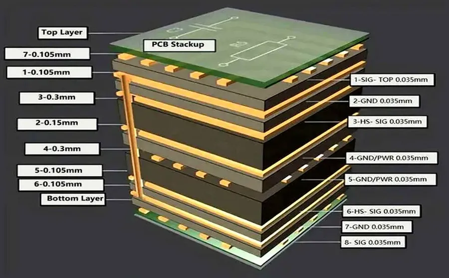
The number of layers in a printed circuit board (PCB) and the intricacy of its design are pivotal determinants of its fabrication cost. As layer count and design complexity increase, so do the manufacturing expenses due to the more intricate processes and higher material consumption involved. Understanding this relationship is crucial for balancing functionality requirements with budgetary constraints.
| Factor | Impact on Cost | Manufacturing Complexity | Typical Applications |
|---|---|---|---|
| Increased Layer Count | Higher | Significantly Increased | Complex electronics, high density routing |
| Complex Routing (e.g. fine pitch) | Higher | Increased | High-speed digital systems, fine-line components |
| High Density Design | Higher | Increased | Miniaturized devices, compact modules |
| Blind and Buried Vias | Higher | Significantly Increased | Multi-layer PCBs with complex interconnects |
| Impedance Control | Higher | Increased | High-speed digital signals, RF applications |
Each additional layer in a PCB requires separate imaging, etching, and lamination steps. Multilayer boards also demand precise alignment and increased complexity when dealing with vias (interlayer connections), especially when blind or buried vias are needed.
Complex routing, characterized by fine pitch and high density designs, necessitates the use of more advanced manufacturing techniques and equipment, which adds to the fabrication cost. Impedance controlled traces and differential pairs, often required in high-speed applications, also increase manufacturing cost due to additional accuracy and control requirements.
Surface Finish Options and Their Cost Implications
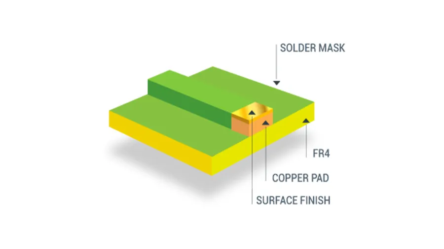
The surface finish of a printed circuit board (PCB) is a critical factor that impacts its solderability, reliability, and overall cost. Different surface finish options offer varying levels of performance and protection against oxidation and corrosion, thus influencing their suitability for specific applications and manufacturing budgets. Selecting the appropriate finish is a balancing act between performance needs and cost considerations.
| Surface Finish | Cost | Benefits | Limitations | Typical Applications |
|---|---|---|---|---|
| HASL (Hot Air Solder Leveling) | Lowest | Good solderability, widely available, robust | Uneven surface, not ideal for fine pitch components, leaded (lead-free available) | General-purpose, through-hole components |
| ENIG (Electroless Nickel Immersion Gold) | Highest | Excellent solderability, flat surface, good for fine-pitch components, good oxidation and corrosion resistance | Most expensive, 'Black Pad' issues if not done correctly | Fine-pitch SMT components, high-reliability applications |
| OSP (Organic Solderability Preservative) | Low to Moderate | Flat surface, good for fine pitch, lead free, relatively low cost | Short shelf life, sensitive to handling, not very robust | General SMT assembly, lower cost applications |
| Immersion Tin | Moderate | Good planarity, lead-free, good for fine pitch | Tin whiskers, short shelf life | Fine pitch applications |
| Immersion Silver | Moderate | Good solderability, flat surface, lead-free | Susceptible to corrosion and tarnishing if not handled properly | High frequency applications |
Manufacturing Volume and Cost per Unit
The quantity of PCBs ordered significantly impacts the per-unit cost due to economies of scale. Larger production runs typically result in lower unit prices, while smaller quantities, often for prototypes, incur higher costs per board. This section explores how to leverage this relationship for cost optimization.
| Order Quantity | Typical Application | Cost per Unit | Setup Costs | Key Considerations |
|---|---|---|---|---|
| 1-10 | Initial Prototypes, Design Validation | High | Low | Focus on Design Iteration, Quick Turnaround |
| 10-100 | Small Batch Prototypes, Pilot Runs | Medium-High | Medium | Moderate cost, good for design verification |
| 100-1000 | Small Production Runs, Early-Stage Products | Medium | Medium-High | Improved efficiency, better per-unit cost |
| 1000+ | Mass Production, Large Scale Rollouts | Low | High | Economies of scale, optimized production |
The above table presents a general overview. It is important to note that specific pricing and cost breaks will vary significantly among manufacturers and depend upon the technology, materials, and complexity of the PCB.
Lead Time and Expedited Manufacturing Costs
Production lead time significantly impacts PCB fabrication costs, with shorter lead times often demanding higher prices due to the need for expedited processing and resource allocation. Understanding the relationship between lead time and cost is crucial for effective budgeting and project management. Standard lead times typically provide the most cost-effective solution, while expedited services cater to urgent requirements at a premium.
Expedited manufacturing, characterized by rapid turnaround, involves prioritizing a specific PCB order within the manufacturing queue. This may involve overtime work, dedicated machine time, and express shipping methods which result in increased cost. The demand for expedited services can stem from time constraints like product launches, critical prototypes, or unexpected production delays.
| Factor | Standard Lead Time | Expedited Lead Time |
|---|---|---|
| Cost | Lower | Higher |
| Turnaround Time | Longer | Shorter |
| Resource Allocation | Standard | Prioritized |
| Manufacturing Process | Routine | Accelerated |
Frequently Asked Questions About PCB Fabrication Cost
Understanding the costs associated with PCB fabrication can be complex due to the many variables involved. This section addresses common inquiries regarding PCB fabrication costs, providing clear, concise answers based on industry best practices and data.
- How can I estimate PCB fabrication costs?
PCB fabrication costs are influenced by factors including board size, layer count, material type, surface finish, and order volume. Most manufacturers provide online tools or quoting systems where you can input your design specifications and receive an estimated price. For preliminary estimates, consider using PCB cost calculators, many of which are available for free online. These tools often allow you to adjust parameters like board dimensions, number of layers and material to get an idea of how these factors affect cost. For more precise estimates, always consult with your chosen manufacturer directly. - How much does it typically cost to manufacture a PCB?
The cost of manufacturing a PCB varies significantly. Simple, single- or double-layer PCBs with standard materials and minimal surface finish can cost as little as a few dollars per board in large quantities. More complex, multilayer boards using exotic materials and advanced surface finishes can cost tens or even hundreds of dollars per board. Prototype quantities typically have higher per-unit costs due to setup fees, and costs per unit decrease significantly with larger order volumes. A small batch of simple PCBs for prototyping might cost $50 - $100 each, whereas a mass production run of the same board could bring the cost down to $1 - $5. - What is a reasonable budget for a PCB project?
Budgeting for a PCB project requires a careful consideration of various factors, including the complexity of the design, the materials to be used, and the quantity of boards required. Start by identifying the necessary performance specifications, then explore the various material and design options that can meet your needs at different cost points. Request quotations from multiple PCB manufacturers to compare pricing and lead times. Consider that prototyping may involve higher costs, and try to balance desired performance with budget constraints. - How does layer count affect PCB fabrication costs?
The number of layers in a PCB significantly impacts the manufacturing cost. Each additional layer requires more processing steps, including additional material, imaging, etching, and lamination, resulting in a cost increase. Multilayer PCBs are necessary for complex designs and higher signal density, but should be carefully evaluated against the added fabrication costs. A double sided board will generally be the least expensive. - Are there cost-effective PCB material options available?
While the standard FR-4 is a cost-effective and versatile option for many applications, alternative materials can be used to lower the cost. For less demanding applications, consider materials with lower thermal or electrical properties. However, it's essential to ensure that the chosen material meets your requirements for performance and reliability. For example, you may be able to choose a lower-cost material that is still sufficient for your application, rather than paying for a higher-end material that you may not need. Consult with manufacturers on material options. There may be a price break for using FR4 materials that are commonly used, compared to other less used materials. - How does PCB surface finish affect cost and performance?
The surface finish of a PCB protects the copper and allows for proper soldering. The choice of finish impacts both cost and performance. HASL (Hot Air Solder Leveling) is among the most cost effective, but may not be suitable for fine-pitch components. ENIG (Electroless Nickel Immersion Gold) provides better surface planarity and is more suitable for advanced components, but it costs more than HASL. OSP (Organic Solderability Preservative) is also a cost-effective option with good solderability but may require more care in handling. Choose the finish that best balances your needs for solderability, longevity, performance, and cost. - What is the impact of lead time on PCB fabrication cost?
Lead time, which refers to the manufacturing turnaround time, has a direct impact on cost. Standard lead times are usually the most economical, while expedited manufacturing services can significantly increase cost. This premium for faster turnaround is due to the manufacturers having to re-prioritize manufacturing queues and adjust to rush orders. If possible, plan your project with sufficient time to avoid the higher costs associated with expedited production.
Optimizing PCB Design for Cost Efficiency
Achieving cost-effective PCB fabrication requires a holistic approach that extends beyond material selection and volume considerations. It begins with strategic design choices that minimize complexity, optimize material usage, and facilitate efficient manufacturing processes. These design-driven optimizations can significantly reduce overall project expenses and lead to long-term savings.
- Design Simplification
Reducing the complexity of your PCB layout is paramount for cost optimization. This involves minimizing the number of vias, layers, and intricate routing paths. A simpler design translates to easier manufacturing and reduced production time. - Standard Component Utilization
Favoring commonly available components over specialized or rare parts not only reduces component costs but also simplifies procurement and ensures quicker turnaround times. Standard components often benefit from volume discounts, further lowering overall expenses. - Material Optimization
Careful consideration of the PCB material is essential. For applications that do not demand high-performance materials, such as FR-4, employing more cost-effective alternatives can substantially reduce expenses. Optimizing material thickness and panelization layouts can also contribute to better material utilization and minimize waste during the manufacturing process. - Strategic Sourcing
Engaging with multiple PCB manufacturers and suppliers allows for competitive pricing negotiations. Building a strong relationship with a reliable manufacturer can lead to reduced costs, faster turnaround times, and superior manufacturing quality. Explore both domestic and international options to determine the most cost-effective choice based on project requirements. - Panelization Optimization
Carefully plan the PCB layout on a production panel to maximize the number of PCBs per panel. This reduces material waste and overall production cost. Work with your manufacturer to understand their panel sizes and processes, to ensure optimal nesting and minimum panel waste. - Design Rule Checks
Thoroughly apply Design Rule Checks (DRCs) to identify potential manufacturing issues in the design phase. Resolving these problems before fabrication reduces the risk of costly re-spins and delays. Design for manufacturability is paramount.
Navigating PCB fabrication costs requires a deep understanding of design, material, and production variables. By carefully considering these factors, you can optimize your design and reduce unnecessary expenses without compromising quality. With the right planning and vendor selection, you can effectively control your PCB fabrication cost and bring your electronic projects to market within budget and on time. Always consider the long-term cost benefits of a robust design against the initial PCB fabrication cost. Understanding the variables that drive costs empowers you to make informed decisions, ultimately maximizing your return on investment.