Finding Your Ideal Single PCB Manufacturer: A Comprehensive Guide with JLCPCB

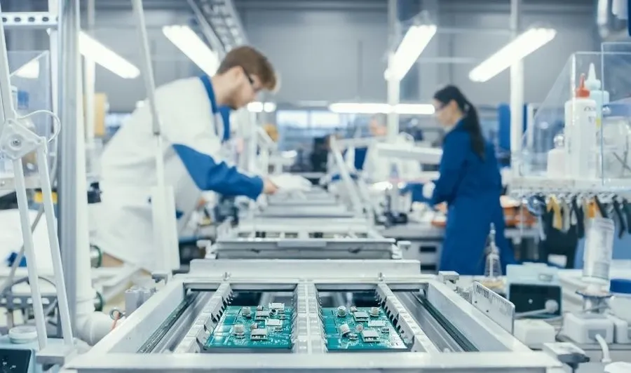
In today’s rapidly evolving electronics landscape, the need for custom printed circuit boards (PCBs) is greater than ever. Whether you're a hobbyist crafting a unique project or a startup developing cutting-edge technology, finding a reliable single PCB manufacturer is crucial. Just as a single thread weaves a tapestry, a single PCB can power a groundbreaking device. This article delves into the world of single PCB manufacturing, guiding you towards making informed decisions and showcasing how manufacturers like JLCPCB meet diverse PCB needs, ensuring the creation of both prototypes and functional devices.
Understanding Single-Sided PCBs
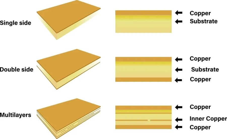
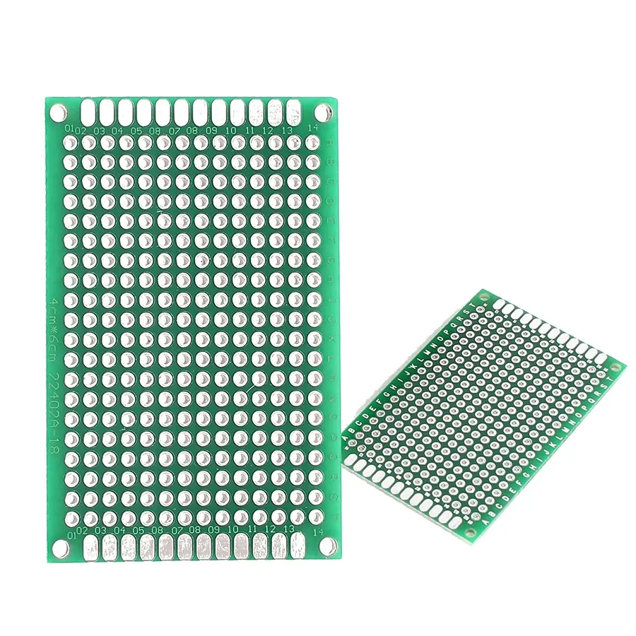
Single-sided printed circuit boards (PCBs) are fundamental in electronics, characterized by having conductive copper traces on only one side of the board, which makes them simpler and more cost-effective than their multi-layer counterparts. This simplicity lends itself to a wide array of applications where complexity and density are not primary concerns, making them a staple for many projects.
- Core Characteristics
Single-sided PCBs feature a single layer of conductive material (typically copper) on one side of a dielectric substrate, such as FR-4. This design limits component placement and routing possibilities to a single plane. - Cost Efficiency
Due to their straightforward construction with less material consumption and simpler manufacturing process, single-sided PCBs are typically more cost-effective than double-sided or multilayer PCBs, making them suitable for budget-conscious projects. - Common Applications
They are widely used in low-density and less complex electronic devices, such as LED lighting, consumer electronics, simple sensor circuits, and basic control systems. - Design Simplicity
The design process for single-sided PCBs is often less complex, which shortens design cycles and reduces time to market, especially for beginners or projects with relaxed space constraints. - Limitations
While cost-effective and simple, single-sided PCBs can limit circuit complexity and density, as they lack the capability for through-hole connections and require careful component placement to avoid shorts.
Key Factors When Selecting a Single PCB Manufacturer
Selecting the right manufacturer for your single-sided PCBs is crucial for project success. The decision hinges on several key factors that directly impact the final product's quality, cost, and delivery timeline. Ignoring these elements can lead to costly delays and unsatisfactory results. A thorough assessment of these factors, as outlined below, will guide you to a manufacturer that aligns with your specific needs and project requirements.
- Cost-Effectiveness
Analyze the pricing structure, including tooling costs, per-unit costs, and potential volume discounts. A manufacturer offering competitive pricing without compromising quality is essential for budget-conscious projects. Seek transparent pricing with no hidden fees. - Lead Time
Evaluate the manufacturer's typical turnaround time for production and delivery. Lead time can vary significantly depending on the manufacturer's capacity, complexity of the design, and order volume. Timely delivery is paramount to keeping your project on schedule. - Quality Standards and Certifications
Confirm the manufacturer's adherence to industry standards, such as IPC (Association Connecting Electronics Industries) standards. Look for certifications and quality control measures that ensure the reliability and performance of the manufactured PCBs. These certifications indicate a commitment to quality. - Manufacturing Capabilities
Assess if the manufacturer has the capability to handle your project's specifications, including board size, material thickness, and minimum trace width/spacing. It is important to choose a manufacturer that has the right equipment and expertise. Verify their machinery is capable of achieving required design specifications. - Customer Support and Communication
Ensure that the manufacturer provides responsive and reliable customer support. Effective communication channels facilitate smooth project execution by quickly addressing any issues or queries that may arise. A dedicated support system proves invaluable throughout production. - Minimum Order Quantity (MOQ)
If you need a small batch, check the minimum order quantity requirement. A low or flexible MOQ is crucial for prototypes or low-volume runs to avoid unnecessary costs. Understanding MOQ prevents overstocking or cost inefficiencies. - Material Options
Review the types of materials available. Common choices include FR-4, CEM-1, and aluminum substrates. Selection of material often influences a pcb's performance and operational environment. Consider material requirements based on project use.
JLCPCB: A Leading Single PCB Manufacturer
JLCPCB stands out as a prominent single PCB manufacturer, particularly recognized for its rapid prototyping capabilities, commitment to high-quality production, and cost-effective solutions, especially beneficial for small batch runs. Their services cater effectively to the needs of diverse designers, from hobbyists to professionals.
JLCPCB's strengths as a single-sided PCB manufacturer can be categorized as follows:
- Rapid Prototyping
JLCPCB offers expedited services, allowing designers to quickly iterate and test their PCB designs. This is critical for fast-paced projects and rapid development cycles. - High Quality
Using advanced manufacturing techniques and stringent quality control measures, JLCPCB ensures high reliability and performance of the final PCBs. This quality is maintained across all batch sizes, from single prototypes to small production runs. - Cost Effectiveness
JLCPCB is known for its affordable pricing, especially for single-sided PCB prototypes and small production quantities. This makes it accessible for smaller projects and educational purposes, without compromising on quality. - Small Batch Production
JLCPCB is particularly adept at handling small batch PCB orders, which is often a challenge for larger manufacturers. This flexibility is ideal for projects requiring limited initial production runs, which is why many designers will choose JLCPCB.
Understanding why JLCPCB is often favored involves a closer look at their manufacturing process, which guarantees accuracy and consistent results. Their online platform allows for easy upload of design files, instant quotes, and efficient tracking of orders, further streamlining the production process for designers. They are especially well suited to users who are designing single-sided PCBs for prototypes and do not require more complex, multi-layer boards. Their customer support is also designed to ensure a smooth process for first-time users.
Single PCB vs. Multi-Layer PCBs: Making the Right Choice
The selection between single-layer and multi-layer PCBs is a critical decision in electronic design, directly impacting project complexity, cost, and performance. Single-layer PCBs, with conductive material on only one side, are simpler and more cost-effective, while multi-layer PCBs offer enhanced routing capabilities and greater density for complex applications. Understanding the distinctions is essential for selecting the most suitable option for each unique project.
| Feature | Single-Layer PCB | Multi-Layer PCB |
|---|---|---|
| Complexity | Simple | Complex |
| Cost | Lower | Higher |
| Layer Count | One conductive layer | Two or more conductive layers |
| Routing | Limited routing options | Extensive routing flexibility |
| Size and Density | Less compact | Higher component density |
| Signal Integrity | More susceptible to noise | Improved noise immunity |
| Applications | Basic circuits, simple devices | Complex electronic devices, high-density circuits |
For instance, a simple LED circuit would typically utilize a single-layer PCB for its straightforward design and low cost, whilst a smartphone or computer motherboard will invariably require a multi-layer PCB to manage the complex signal routing, high component density, and sophisticated functionality. The advantages and disadvantages of each type directly influence whether they align with project objectives.
Design Considerations for Single-Sided PCBs
Designing single-sided PCBs requires a meticulous approach, balancing functionality with the inherent limitations of having conductive traces on only one layer. Optimal layout and component placement are paramount to ensure efficient and reliable operation while minimizing manufacturing complexities. Adhering to specific design rules tailored to single-sided boards is essential to avoid issues during fabrication and assembly.
- Layout Considerations
Prioritize component placement to minimize trace lengths and the need for vias. Group related components together to streamline signal flow and reduce electromagnetic interference. Consider the physical dimensions of components and their heat dissipation requirements during layout to ensure proper function and reliability. - Component Placement
Carefully orient components to facilitate routing on a single layer, placing larger components in areas that can accommodate their size and heat dissipation. Ensure adequate spacing between components to avoid interference during assembly and operation. Choose component footprints appropriate for manual or automated assembly processes. - Trace Routing
Minimize trace lengths and avoid sharp angles to reduce signal reflections. Employ a grid-based approach to maintain spacing and ensure consistent impedance. Use wider traces for power and ground signals to improve current handling capabilities and reduce voltage drops. - Design Rule Checks
Adhere to minimum trace width, spacing, and via size specifications as dictated by your manufacturer. Consider manufacturability when selecting via sizes and pad shapes, minimizing fabrication costs. Conduct thorough design rule checks before submitting design files to identify and correct any violations.
| Design Parameter | Consideration for Single-Sided PCBs |
|---|---|
| Trace Width | Sufficient width to handle current without excessive heating. Use wider traces for power and ground. |
| Trace Spacing | Adequate spacing to prevent shorts and ensure manufacturability, consider manufacturer's minimum specifications. |
| Via Size and Placement | Minimize vias where possible. Ensure via sizes are suitable for manufacturing, and that they do not interfere with traces or components. |
| Component Orientation | Orient components to simplify trace routing on a single layer. |
| Heat Dissipation | Strategic component placement to facilitate proper heat management, utilizing heat sinks and thermal vias if needed. |
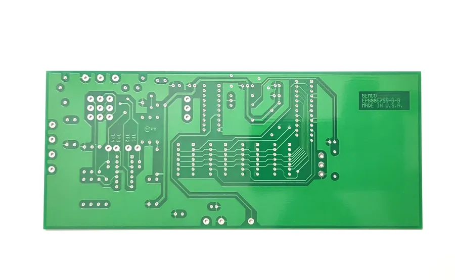
The PCB Manufacturing Process
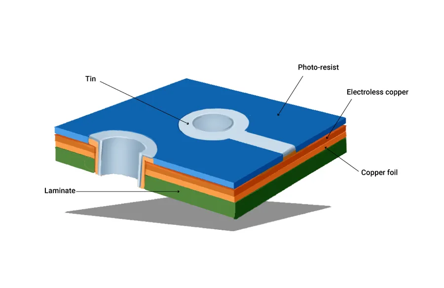
The manufacturing of single-sided PCBs involves a sequence of precise steps to transfer a design into a functional circuit board. This process, often streamlined by manufacturers like JLCPCB, includes design preparation, material handling, imaging, etching, drilling, and quality control, ensuring consistent production of reliable PCBs.
- Design Preparation
The process begins with the design of the PCB layout, typically using specialized software. The design files (Gerber files) are then prepared for manufacturing, ensuring all specifications are met. - Material Handling
A base material, often a rigid substrate like FR-4 (a fiberglass epoxy laminate), is selected. This material is coated with a thin layer of copper on one side. - Imaging
A photoresist layer is applied over the copper surface. Using a photolithographic process, the circuit pattern is transferred to the photoresist. This involves exposing the resist to UV light through a film mask of the PCB design, which hardens the exposed areas. - Etching
The unhardened photoresist is then washed away, and the board is submerged in an etching solution. This chemical process removes the exposed copper, leaving behind the desired copper traces that form the circuit. - Drilling
Holes for component insertion and mounting are precisely drilled using automated machines. These holes are drilled according to the PCB design specifications. - Solder Mask Application
A solder mask, typically a green protective layer, is applied to the board, exposing only the areas intended for soldering. This mask prevents solder bridges and protects the copper traces. - Silkscreen Printing
Component labels and other designators are printed on the solder mask using a silkscreen process, aiding in assembly and testing. - Surface Finish
A final surface finish, such as HASL (Hot Air Solder Leveling) or ENIG (Electroless Nickel Immersion Gold), is applied to the exposed copper pads to prevent oxidation and ensure good solderability. - Quality Control
Each board undergoes a thorough inspection for dimensional accuracy, connectivity, and overall quality. Electrical tests may also be performed to verify functionality.
Frequently Asked Questions about Single PCB Manufacturing
This section addresses common questions and clarifies misconceptions about single-sided printed circuit board (PCB) manufacturing, providing practical insights into their design, production, and cost-effectiveness.
- How are single-sided PCBs manufactured?
Single-sided PCB manufacturing typically involves a process of applying a copper layer to one side of a substrate material (like FR4). The desired circuit pattern is then created through a photolithographic process where a photoresist is exposed and developed, followed by etching away unwanted copper. Finally, drilling, solder mask application, and component marking are performed. - Who is the best PCB manufacturer for single-sided boards?
The 'best' manufacturer depends heavily on the user's specific requirements. For rapid prototyping, manufacturers like JLCPCB offer cost-effective and quick turnaround times, often ideal for single-sided boards. However, for high-volume production, other manufacturers may be more suitable based on capacity and specific capabilities. It is imperative to evaluate factors such as quality, price, lead time and minimum order quantity (MOQ). - Are single-layer PCBs generally cheaper than multi-layer PCBs?
Yes, single-layer PCBs are generally less expensive than multi-layer PCBs. This cost difference arises from their simpler manufacturing process and fewer material requirements. They only have copper on one side, which reduces materials and processing steps. Single-sided PCBs are most cost effective where complexity is not a major concern. - What are the typical applications for single-sided PCBs?
Single-sided PCBs are commonly used in simpler electronic devices, including many low-complexity circuits, such as LED lighting systems, basic power supplies, sensors, and simple control boards. They are a popular option in situations where complex routing is not needed, and cost-effectiveness is a high priority. - Is it possible to get a single PCB prototype made quickly?
Yes, many manufacturers, including JLCPCB, offer rapid prototyping services specifically catering to small batch orders and prototyping. This rapid service typically involves expedited manufacturing and shipping, getting your designs in your hands much faster, often within a few days. - What are the key differences between single-sided and double-sided PCBs?
The main difference is the copper layer, with single-sided PCBs having it only on one side, limiting component placement and routing possibilities. Double-sided PCBs, in comparison, offer copper layers on both sides, which allows for more complex designs and increased routing flexibility and density. - What are some common misconceptions about single-sided PCBs?
A common misconception is that single-sided PCBs are always of lower quality than multi-layer PCBs. While they are simpler, when manufactured correctly they offer excellent reliability and are suitable for many applications. Another misconception is they are less versatile, when the single sided design is used creatively, they are ideal for many types of electronic applications. Finally, some think that only multi-layer PCBs can deliver optimal performance, but for many applications the use of single sided PCB's greatly reduces both the cost and time for the manufacture of the PCB.
Cost-Effective Solutions for Single PCB Prototypes
Optimizing the cost of single PCB prototypes involves a multi-faceted approach, focusing on design efficiency, material choices, and leveraging manufacturer capabilities like JLCPCB. By strategically addressing these aspects, significant cost reductions can be achieved without compromising functionality or quality.
- Design Optimization for Cost Reduction
Streamline your PCB layout by minimizing board size and utilizing only the necessary components. Reducing the complexity and size of your board directly impacts material usage and manufacturing time, translating into cost savings. Employing single-sided design when feasible over multi-layer boards can also reduce production costs significantly. - Material Selection
Choose cost-effective materials for your PCB, such as FR-4, which is widely used for its balance between performance and price. Avoid specialized, expensive materials unless the application strictly requires them. Consider the environmental requirements, and select the most economical material that meets your project needs without overspending on higher-performance but more expensive alternatives. - Component Selection
Selecting commonly available and affordable components reduces the procurement costs of your project. Ensure that the components are easily sourced and have minimal lead times for faster production. Standard components often have better economies of scale, directly reducing the costs compared to high-end or custom parts. - Panelization and Batching
Panelizing multiple boards on a single manufacturing panel reduces the per-board setup and handling costs. Consider ordering boards in batches to benefit from economies of scale, especially from manufacturers like JLCPCB who offer volume discounts, which translates into lower per-unit prices. Combining orders with similar designs can also lower costs. - Utilizing Manufacturer Discounts and Services
Take advantage of promotional offers and discounts often provided by manufacturers like JLCPCB for prototypes or bulk orders. Many manufacturers provide free design rule checks and DFM (Design for Manufacturing) services, which can help you catch errors and optimize your design for reduced production cost before actual manufacturing. Always compare quotes from different suppliers to ensure competitive pricing and maximize cost-effectiveness of your prototypes.
Finding the right single PCB manufacturer, like JLCPCB, is paramount for your project's success, whether for rapid prototyping or small batch production. By understanding your needs and carefully evaluating manufacturer capabilities, you can ensure high-quality, cost-effective PCBs that will bring your designs to life. As technology continues to advance, it is essential to choose a partner that can adapt to the increasing complexity and precision required in PCB fabrication. The future of innovation relies on reliable PCB manufacturers and their capabilities to meet the demands of a dynamic industry.