High Multilayer PCB Manufacturing Process Flow
•
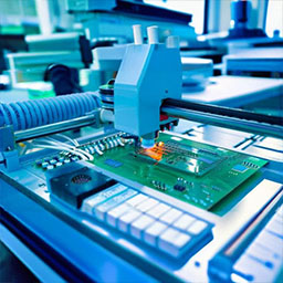
AnyPCBA
High multilayer PCB can provide more alignment layers, so that the circuit design is more complex and dense, so as to meet the needs of high-frequency and high-speed transmission. Moreover, high multilayer PCBs can also achieve better signal integrity and electromagnetic compatibility. This is particularly important for high-end applications such as 5G communications, high-performance computing, and automotive electronics. Therefore, high multilayer PCB has become one of the important trends in the future development of the PCB industry. For PCB design engineers or electronic hardware design engineers, it is also necessary to understand the manufacturing process related to high multilayer PCB.
High multilayer PCB is not just an increase in the number of layers, its manufacturing difficulty has increased exponentially. Compared to single-layer, double-layer boards, high-multilayer PCB manufacturing will also need to pay attention to the inter-layer connection, inter-layer stacking and alignment and precise pressure control and other process control, PCB in the design of the signal integrity and electromagnetic interference and thermal management issues need to be considered in order to take full advantage of the performance of the high-multilayer PCB advantages.
From process, equipment, design capabilities to quality control, collaboration capabilities, high multilayer PCB board manufacturers have higher requirements for the level of manufacturing process. In this article, some key processes about high multilayer PCB manufacturing are introduced.
1. Submit Manufacturing Information
As the beginning of PCB manufacturing, first of all, we need to submit the relevant manufacturing information to the PCB factory.The information and common data formats required for PCB manufacturing include the following:- Gerber file (RS274X format).
Gerber RS274X is the current mainstream format, the output of the Gerber file includes all circuit layers, soldermask layer, solder paste layer, silkscreen (character) layer, board frame, hole-splitting diagrams, manufacturing requirements (such as multilayer board stacked layer structure schematic, interlayer media thickness, impedance control requirements, plug hole requirements, etc.). At the same time, the Gerber file should also be able to facilitate the PCB factory process engineers to identify the layer information corresponding to each Gerber file, so it is recommended to name the Gerber file according to certain naming conventions.
- Drill Files
Drill file contains all the drill coordinates and diameter data, commonly used file format is Excellon format.
- Netlist data
IPC has defined a compatible format, IPC-356, that provides all the information necessary to generate netlist and electrical performance test data. Complete PCB documentation is very important for the manufacturing of multilayer PCBs as compared to single or double sided boards, the most important information in the manufacturing information document is:
1. Complete layer structure
2. Precise information about the substrate
3. High-frequency and high-speed boards also need to provide the substrate manufacturer and product name
4. Impedance control requirements
5. Special process instructions (e.g. hole plugging requirements)
2. Manufacturing Information Audit
PCB board factory audit of manufacturing information is aimed at determining the approximate manufacturing costs, and to prepare for manufacturing. Proper pre-analysis before a product is manufactured or processed can save time and material. it is the PCB fab's responsibility to determine if its process capabilities can accommodate a given product.PCB factory will adjust the PCB design according to its manufacturing process wiring information, such as over-hole drilling diameter compensation or alignment etching compensation, etc., in order to improve PCB manufacturability, some critical modifications to the board factory will also be communicated with the PCB Layout to confirm that, of course, the more ideal situation is, in the process of PCB design process on the consideration of the DFM manufacturability and design optimization, which will save a lot of late with the PCB factory to confirm. This will save a lot of time to communicate with the PCB factory later to confirm.
If the board is made in Garrigon, they also provide a personalized service of “Confirmation of Production Draft” as an option, as long as we carefully check the confirmation, we can find out the problems on our own design, and of course, we can also find out some of the errors in the process of Garrigon's engineers. Don't forget to ask the engineer to refund the production confirmation fee if the problem is caused by Garrigon.
3. Material Preparation
Unlike single- and double-sided boards, which are manufactured directly from copper-clad laminates that meet the thickness requirements of the final product, multilayer boards are different. Multilayer boards have multiple copper layers in the board structure and therefore require special substrates to manufacture. The creation of multilayer boards requires the use of a combination of semi-cured sheets (PP) and relatively thin copper-clad laminates (Core boards) that are pressed and cured to the final thickness. The laminate structure depends on the electrical parameters, which are determined by the PCB designer in consultation with the board manufacturer and planned well in advance of the PCB Layout to meet the line width/spacing requirements for the specific impedance.Due to the different laminate structures, there are various thicknesses of semi-cured sheets to meet different transmission line and power plane combinations. Each type of semi-cured sheet consists of a designated fiberglass braid type with a number, such as 1080, 2116, 3313, or 7628. the following figure gives the identification of this type:
The second component of a multilayer circuit board is a relatively thin copper-clad laminate (as opposed to the copper-clad laminates used to make single- and double-sided PCBs), also known as a core board. It is a fully cured substrate covered with copper foil on one or both sides. Of course, it is also available without copper and is called bare board.
The core board is actually made up of semi-cured sheets and copper foils that are laminated together and manufactured by the substrate supplier, who, according to IPC-4101 specifications and market demand, selects semi-cured sheets with different weave styles of fiberglass cloth and resin content, and copper foils with specified specifications, and then presses them together to produce different specifications of copper-clad laminates.
The manufacturing of multi-layer circuit boards is completed by the PCB factory, but the substrate is provided by the substrate manufacturer, it should be noted that there are many kinds of substrate specifications, each PCB factory's substrate reserves are also different, if the PCB laminated design needs to be used to the special specifications of the semi-cured sheet as well as the core board, it is best to communicate with the PCB factory in advance to learn about the substrate's supply cycle.
Choosing good raw materials to make a good performance of the PCB, the board in the PCB manufacturing process plays a key role in the performance and reliability of the PCB has an important impact on the performance and reliability of the PCB, including electrical performance, thermal performance, mechanical strength, processing performance and environmental adaptability.
In terms of boards, Garrison uses raw materials from large manufacturers. For 4-layer and 6-layer boards, Garrigon uses KB and Taiwan South Asia boards, which are of high quality and guaranteed. KB boards use high-quality fiberglass-reinforced epoxy resin (FR-4) as the substrate, and high-purity copper foil as the conductive layer, and undergo a rigorous process, so they have the characteristics of high quality and good performance, and are widely used in the electronics industry.
And China Taiwan Nanya is also well known in the market, which provides boards with not only good electrical properties, high strength and rigidity, but also high temperature and chemical resistance, which can improve the reliability and life of the products.
For 8-layer boards and higher, Garrison uses Nanya and Sang-Yi boards from Taiwan, China. Among them, as a well-known supplier of copper-clad laminates in China, SangYi's laminates are characterized by high standard, high quality, high performance and high reliability, which are highly recognized in the industry and are widely used in industrial control, medical instrumentation/devices, consumer electronics, automotive and other electronic products.
4. Manufacturing process of multilayer boards
As shown in the above figure of the multilayer board production process, the manufacturing of multilayer boards and single-double-sided PCB manufacturing compared to more than one inner layer of the process flow, the key step is the inner layer of the laminated compression process control, which is critical for the controlled impedance of the electrical performance of the transmission line. After the completion of the inner layer process lamination, came to the same manufacturing process with the manufacture of single and double-sided boards, until the final inspection process.The manufacturing process for multilayer boards, when broken down, typically requires about 200 different processing steps. Therefore, it is very important for PCB designers to familiarize themselves with the different types and properties of substrates, the manufacturing process of multilayers and the soldering process. By combining different sizes of semi-cured sheets and copper-clad laminates (core boards), all required thicknesses can be achieved. For the laminated structure of multilayers, care needs to be taken that the individual layers must be symmetrical and have the same layer thickness. The copper of the inner layers should be evenly distributed over these symmetrical layers. If the distribution is not uniform, the uneven thermal stress during heating will cause the board to warp.
One of the factors that has a great impact on the quality of a multilayer board structure is the precise alignment of the individual layers. The layers must overlap precisely, otherwise the circuits between the layers may suffer from open-short problems after being connected by drilling holes. The layers are precisely adjusted by mechanically aligning the holes and then using locating pins to adjust the layers as they are laminated. To ensure a good bond between the internal layers and the semi-cured sheet, the copper surface must be chemically roughened, a roughening process known as browning. Inspection of the internal circuit layers prior to press-fit of the multilayer printed circuit boards is essential to ensure quality. At this stage, if the inspection reveals connections or other defects, they can still be repaired, and the inspection is usually automated using AOI (Automated Optical Inspection), an AOI system that provides a direct visual comparison of the etched circuit graphics with the CAD data.
The above figure is the press-fit manufacturing schematic of a 6-layer rigid multilayer board, A1, A2, A3 are semi-cured sheets, L2-L3, L4-L5 are double-sided copper-clad laminates for completing the inner layer of the graphic, and B1, B2 are copper foils for the outer layer of the circuit.
The principle of conventional rigid multilayer board pressing is to combine a certain number of double-sided copper-clad laminates (the inner layer of the graphic has been completed and browned to strengthen the bonding force), double-sided copper-clad laminates are separated by a semi-cured sheet, which serves as an insulating material to avoid short-circuiting of the various copper layers, and at the same time, the semi-cured sheet is heated, in which the resin will be melted to achieve the bonding of the various copper-clad laminates again. Finally, the laminates are connected through metallized holes. Currently Garritron's multilayer manufacturing process can produce up to 32 layers of multilayers, which is sufficient to cover most applications.
Precise control of the press-fit is critical to the impact of the characteristic impedance of the controlled impedance transmission line. During the press-fit process, as the temperature rises, the epoxy resin in the semi-cured sheet re-melts, and it fills in the gaps between the wires by flowing and bonding the inner layers together. The flow characteristics of the resin affects the distance between the final signal layer and the reference layer, and changes in the distance between the signal layer and its reference layer have the The change in the distance between the signal layer and its reference layer has the greatest impact on the change in impedance.
As shown in the figure above, the PCB design is ultimately assembled to a large working panel for production, for the characteristic impedance control, the entire large panel in the press, the uniformity of resin flow for the impedance change of the impact can not be ignored, this time the performance of the press equipment used will be critical.
Equipment is one of the most important factors affecting the quality of high multilayer. For this reason, Garrigram adopts the industry's first-class equipment to produce high-multilayer panels to ensure product quality.
Garrison uses the latest generation of fully automatic laminating machine from Vigor of Taiwan, China, which is more stable and has better laminating quality. As a professional PCB equipment provider, Vigor's laminating machine has high precision, high reliability and advanced control system, which can satisfy the stacking and laminating of PCB high multilayer boards.
After the press-fit is completed, it comes to the drilling process, followed by the same process flow with single and double-sided boards, but also slightly different, such as Jialichuang, their family for the manufacture of high-multilayer boards, but also launched a free to enjoy the services to improve the quality of the PCB.
One is to enhance the immersion gold process, Jialichuang 6-32 layers of circuit boards all use immersion gold process, and immersion gold thickness of free upgrade to 2u”. Immersion gold is a relatively expensive surface treatment in the industry, which can provide good electrical connection, corrosion resistance and soldering performance. The gold immersion layer provides a smooth, uniform metallic surface that helps maintain good signal transmission and impedance control. Moreover, it ensures the stability and durability of the metal layer during the soldering process, providing excellent corrosion resistance and extending the life of the PCB.
In addition to the immersion gold process, Garrison uses the hole-in-dish process (resin plugged holes + plated caps) free of charge for all 6-32 layer boards. For the quality of PCB, vias are very important,because they play an important role in electronic devices, supporting the realization of complex circuits and functional reliability. Due to a variety of factors, vias can slowly corrode, leading to connection failures, signal degradation, short circuits and leakage, and reliability issues, which are effectively solved by the hole-in-dish process. In short, the manufacture of multilayer boards relative to single and double-sided boards, not just one more inner layer of the process is so simple, nor is the PCB production directly thrown to the PCB board factory on the end, at least in the PCB design process, we should understand the process capabilities of the PCB board factory in the design of the introduction of the DFM oriented design for manufacturability in the real implementation of the wiring before we need to carry out with the PCB board factory to Communicate to determine the required board and stacking structure to meet the performance requirements of the specific transmission line structure, and can be manufactured at a reasonable cost and time.
October 18, 2024