How to Order Prototype PCBs: A Comprehensive Guide
In today's fast-paced world of electronics development, rapid prototyping of printed circuit boards (PCBs) is crucial for innovation. Ordering a prototype PCB can seem daunting, but it’s a straightforward process when you know the steps. This article guides you through everything you need to consider when you order prototype pcb, ensuring your next project is a success.
Understanding Your PCB Needs Before You Order Prototype PCB
Before initiating the order of prototype PCBs, a precise understanding of your project's specific requirements is paramount. This foundational step ensures that the manufactured boards will meet your design intent and functional needs. Accurately defining these parameters will significantly streamline the selection process and yield precise cost estimations.
- Board Dimensions
Accurately define the length and width of your PCB to ensure proper fit within your project's enclosure and system constraints. These dimensions must be exact to prevent fitment or interference issues. - Layer Count
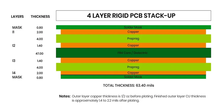
Specify the number of copper layers required for your design. The complexity of your circuit, including signal routing and power distribution, typically determines this. Options range from single-layer boards for simple circuits to multi-layer boards for more complex designs. - Material Type
The standard material for PCBs is FR4 (Flame Retardant 4), which is suitable for most general-purpose applications. However, for high-frequency or high-temperature applications, specialized materials like Rogers or ceramic may be necessary. Selecting the appropriate material ensures the board's performance and reliability. - Copper Thickness
Specify the thickness of the copper layers. Standard thickness ranges from 0.5 oz/ft² to 2 oz/ft². Thicker copper is required for high-current applications, while thinner copper is often sufficient for signal layers. Choosing the correct copper thickness ensures that your circuit meets its current-carrying requirements without overheating. - Impedance Control
If your circuit involves high-speed signals, impedance control is crucial to prevent signal reflections and distortions. This may involve special trace geometries and specific layer stack-ups. In high-speed designs, impedance control maintains signal integrity and improves overall circuit performance. - Special Requirements
Identify any other specific needs such as controlled dielectric thickness, specific surface finish types (e.g., ENIG, HASL), via types (e.g., blind, buried), or thermal management features like heat sinks or thermal vias. These specific needs must be considered to ensure the manufactured PCB meets all design criteria and performance expectations.
Choosing the Right PCB Manufacturer for Your Prototype
Selecting the appropriate PCB manufacturer is crucial for a successful prototyping phase. Numerous manufacturers specialize in prototype PCB fabrication, each offering a unique combination of services, pricing, and technological capabilities. Your choice should be carefully considered based on your specific project needs and constraints.
| Factor | Description | Consideration |
|---|---|---|
| Cost | The overall price per board, influenced by board size, layer count, materials, and quantity. | Evaluate if the cost fits within your budget. |
| Turnaround Time | The time from placing your order to receiving the fabricated PCBs. | Determine if the lead time aligns with your project timeline. |
| Minimum Order Quantity (MOQ) | The smallest number of boards a manufacturer will produce in a single order. | Ensure the minimum quantity meets your prototyping requirements. |
| Technology Availability | The manufacturer's capabilities with specialized technologies like blind/buried vias, impedance control, or HDI. | Confirm the availability of technologies you need for your PCB. |
| Material Options | The variety of substrate materials offered, such as FR-4, Rogers, or aluminum. | Select the materials suitable for your application's thermal, electrical, and mechanical requirements. |
| Surface Finish Options | Options such as HASL, ENIG, or OSP, which affect solderability and corrosion resistance. | Choose the surface finish that best meets your soldering and environmental needs. |
| Quality Standards | The manufacturer's quality control processes, certifications (e.g., ISO 9001), and reputation. | Verify the quality standards of the manufacturer before placing your order. |
| Shipping Options | The shipping methods offered, their transit times, and associated costs. | Evaluate shipping times to determine the impact on project timelines and cost of delivery. |
Popular PCB prototyping manufacturers like PCBWay, JLCPCB, and Seeed Studio are often considered for their balance of cost, turnaround time, and capabilities. However, the best choice depends on your individual project requirements. Thoroughly research and compare several options before committing to a specific manufacturer.
Preparing Your Design Files for Prototype PCB Ordering
Accurate and properly formatted design files are paramount for successful prototype PCB fabrication. Manufacturers rely on these files to produce PCBs that match your design specifications precisely. The most critical file format is the Gerber file, the industry standard for PCB manufacturing data.
- Gerber Files
Gerber files are a set of 2D vector files that define each layer of your PCB design. These layers include copper traces, pads, silkscreen, solder mask, and board outline. Each layer requires its own Gerber file. - Drill Files
A drill file contains the information necessary for the manufacturer to accurately drill holes in your board. It details the location, size, and type of each hole and is usually in Excellon format. - Bill of Materials (BOM)
If you're ordering PCB assembly along with your prototype PCB, you'll need a comprehensive BOM. This includes a list of all components, their part numbers, manufacturer information, and quantities needed.
To ensure your prototype pcb is manufactured accurately, it's essential to verify that the Gerber files are generated correctly from your EDA software such as Eagle, Altium, or KiCad. A Gerber viewer can be used to preview the generated files and confirm all layers are as expected before you upload them to your manufacturer.
The Online Ordering Process for Prototype PCBs
The online ordering process for prototype PCBs has become streamlined, allowing for efficient and convenient procurement. Most manufacturers now offer comprehensive online platforms where users can upload design files, specify board parameters, and receive instant quotations, all within a few minutes. This digitalization has significantly reduced the traditional barriers of entry to PCB fabrication, making it more accessible for everyone from hobbyists to large corporations.
The typical online ordering process for prototype PCBs generally involves several key steps:
- File Upload
Begin by uploading your Gerber files, which are the standard industry format for PCB designs. Ensure all necessary files are included (.GTL, .GBL, .GTS, .GBS, .DRL etc.) and that they are generated correctly from your design software. Some platforms also allow native file uploads from certain EDA software packages. - Specification Selection
Next, specify the required parameters such as PCB dimensions, layer count (single, double, or multi-layer), material type (commonly FR4), copper thickness, surface finish (HASL, ENIG, etc.) and solder mask color. Some may offer additional options such as impedance control, via type (blind, buried) or specific PCB thickness. - Quotation and Review
Once specifications are selected, the system provides an instant quote. Review this breakdown carefully, noting any minimum order quantities (MOQs) and delivery timelines. Some platforms will also provide a cost breakdown per unit. Be aware of any additional charges for custom options or expedited shipping. - Order Placement
If the quote aligns with your budget and timeline, proceed to place the order. This will typically involve payment through a secure online portal, using various credit cards or bank transfers. Verify the accuracy of the order summary before final submission. - Order Tracking
Following order placement, you can usually track its progress via the manufacturer’s website or dedicated app. This includes updates on production, quality check, and shipping.
Cost Factors When You Order Prototype PCB
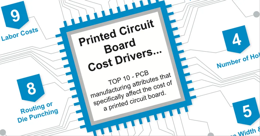
The cost of prototype PCBs is influenced by a multitude of factors, necessitating a strategic approach to design and vendor selection. Understanding these cost drivers is crucial for minimizing expenses while still achieving desired functionality for your initial prototypes. By carefully considering these factors, you can optimize your budget and ensure cost-effective PCB development.
| Cost Factor | Impact on Price | Considerations for Cost Reduction |
|---|---|---|
| Board Size | Larger boards generally cost more due to increased material usage and processing time. | Optimize board size to the smallest functional area. Panelize your design if ordering multiple boards to reduce per-unit cost. |
| Layer Count | More layers increase complexity and manufacturing costs. | Minimize the number of layers where possible; evaluate whether design can be achieved with fewer layers. |
| Material Type | Standard FR4 is typically the most cost-effective material. Specialized materials (e.g., high Tg, Rogers) will increase costs. | Use standard materials for prototypes unless the application absolutely requires special material properties. |
| Copper Thickness | Thicker copper layers are more expensive but may be required for high current applications. | Specify standard copper thickness (e.g., 1 oz) when feasible. |
| Finish Type | HASL (Hot Air Solder Leveling) is often the cheapest finish, while ENIG (Electroless Nickel Immersion Gold) is more expensive but provides better solderability and corrosion resistance. | Use the most cost-effective finish suitable for your prototype requirements; consider HASL for initial testing. |
| Quantities Ordered | Larger quantities generally lead to lower per-unit costs due to economies of scale. | If your prototype uses the same PCB multiple times, consider ordering more to bring the per unit cost down. |
| Special Features (e.g., Impedance Control, Blind/Buried Vias) | These features add significant cost due to increased manufacturing complexity. | Avoid special features in initial prototypes unless required for functional validation. |
| Testing Requirements | Electrical testing can increase the overall cost of each prototype. | Consider if electrical testing is necessary or if you can test the assembled board yourself. |
Quality Assurance and Inspection of Your Prototype PCBs
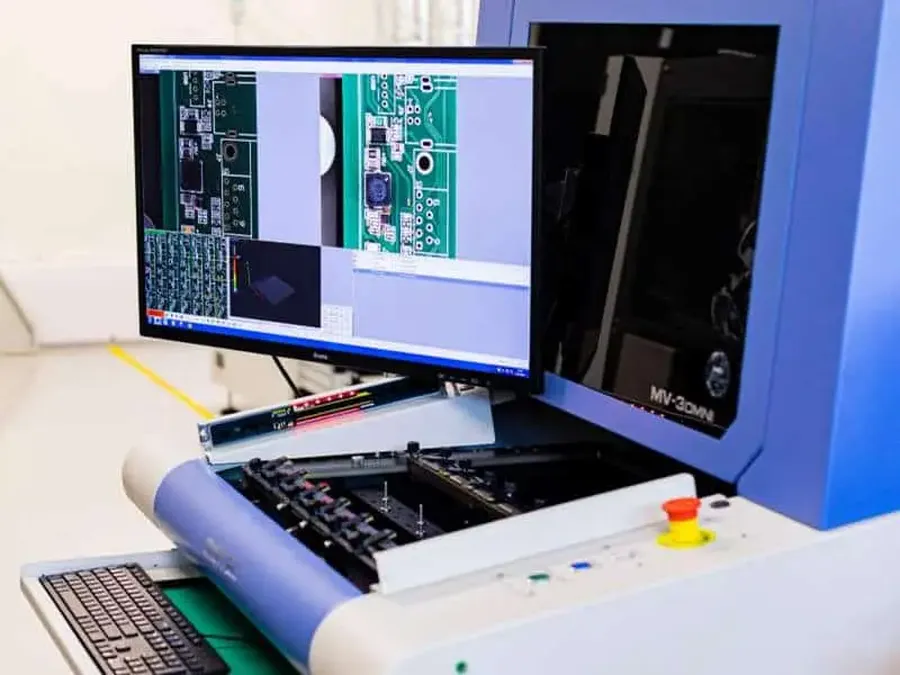
Ensuring the quality of prototype PCBs is critical for the success of any electronic project. This involves not only relying on the manufacturer's quality checks but also conducting your own thorough inspection upon receipt of the boards. This section outlines the key areas to focus on when inspecting your delivered PCBs.
A comprehensive quality report from your PCB manufacturer is a good starting point, but a hands-on inspection is crucial. The following points detail the primary aspects of quality control you should consider when assessing your prototype PCBs:
- Lamination Quality
Examine the board for any signs of delamination or separation of layers. This can be a significant issue that affects the mechanical integrity and electrical performance of the PCB. Look closely at the edges and corners, as these are common locations for lamination defects. Any bubbles, voids, or uneven surfaces could indicate problems. - Via Quality
Inspect the vias for proper plating and alignment. Vias connect different layers of the PCB and are crucial for signal and power integrity. Check for any open vias, missing plating, or misalignment. A lack of plating within the via barrels can lead to unreliable connections. - Silkscreen Accuracy
Verify that the silkscreen, which includes component designators and labels, is accurately placed and legible. Misaligned or unclear silkscreen can make assembly and debugging challenging. Ensure that labels correspond to the design files and are printed clearly. - Solder Mask Application
Confirm that the solder mask is correctly applied, covering all areas except for the pads that are meant to be soldered. Any areas where solder mask is missing or incorrectly applied can lead to solder bridging during assembly. Check for proper alignment and coverage. - Surface Finish
The surface finish on the pads, such as ENIG (Electroless Nickel Immersion Gold), HASL (Hot Air Solder Leveling) or other finishes should be uniform and free from defects. The finish protects the copper pads from oxidation and ensures good solderability. Look for any discoloration, unevenness, or peeling of the surface finish. - Overall Cleanliness
The PCB should be free of dust, debris, and contaminants. Residue from the manufacturing process can cause issues during assembly and operation. Check for any fingerprints, flux residues, or other foreign materials. - Dimensional Accuracy
Verify the dimensions of the board using calipers. Check that the overall size and the locations of mounting holes are accurate. Any deviations from the specified dimensions can result in fitment issues within the enclosure or with other components. - Defect Identification
Look for any apparent defects such as shorts, opens, scratches, or broken traces. These can be visually identified, sometimes with the aid of a magnifying glass. Any such defects would require further investigation.
If any issues are detected, it's essential to communicate them to the manufacturer promptly. Documenting defects with photographs can be helpful. Manufacturers should offer remedies if the prototypes do not meet the required specifications. Depending on the severity of the problem, remedies may include re-fabrication of the boards or a partial refund.
Turnaround Time: How Fast Can You Get Your Prototype PCBs?
Turnaround time, the duration between placing your prototype PCB order and receiving the finished boards, is a critical factor in many projects. This period can vary considerably based on several elements, including the manufacturer's capabilities, the complexity of your design, and the service level you select. Understanding these influencing factors is crucial for effective project planning.
- Factors Affecting Turnaround Time
Several factors can influence the turnaround time for prototype PCBs. These include the complexity of the board design (e.g., number of layers, via types), the materials used, the manufacturer's current workload, and whether you opt for a standard or expedited service. Also, the availability of specific components in the case of PCBA (printed circuit board assembly) can affect the total turnaround time. - Standard vs. Quick Turn Services
Most PCB manufacturers offer both standard and quick-turn services. Standard services are more cost-effective but have longer lead times. Quick-turn services significantly reduce the turnaround time, sometimes down to 24-48 hours for basic PCBs, but come with a premium price. Selecting the right service depends on your project’s timeline and budget constraints. - Typical Turnaround Times
For standard prototype PCB orders, you can expect turnaround times to range from 1-2 weeks. Simple, 2-layer boards can sometimes be produced in a shorter period, while more complex designs with multiple layers or specific material requirements will typically take longer. It is always best practice to check with the manufacturer for the most accurate estimate. - Communicating Deadlines
If time is a crucial factor for your project, it's essential to communicate your deadlines with the manufacturer clearly during the quoting and ordering process. Confirm their typical turnaround time for your specific order details and any potential delays. This will help in your scheduling and allow for any unforeseen issues that might arise.
| Service Type | Typical Turnaround Time | Cost | Suitable for |
|---|---|---|---|
| Standard | 1-2 weeks | Lower | Projects with flexible timelines |
| Quick Turn | 1-5 days | Higher | Urgent prototypes and time-sensitive projects |
Prototype PCB Assembly Considerations
When moving beyond bare boards to a fully functional prototype, PCB assembly (PCBA) becomes a critical step. This process involves the precise application of solder paste, accurate placement of electronic components, and reflow soldering to create reliable electrical connections. Many manufacturers that produce prototype PCBs also offer PCBA services, allowing for a streamlined approach from design to functional prototype. It's essential to understand the key aspects of PCBA before ordering this service alongside your prototype PCBs.
- Solder Paste Printing
Solder paste is applied to the PCB pads using a stencil. The precision of this process is critical for ensuring that the solder joints form correctly during reflow. - Component Placement
Automated machines pick and place surface mount components onto the PCB with high accuracy. Proper alignment and orientation are essential for functional PCBs. - Reflow Soldering
The assembled board passes through a reflow oven, where the solder paste melts, creating a durable and electrically conductive bond between the components and the PCB pads. - Component Availability
Before ordering PCBA, verify the manufacturer's component library and confirm that they can source all necessary parts. Consider providing alternative components if your primary choice is unavailable.
| PCBA Process Step | Description | Key Considerations |
|---|---|---|
| Solder Paste Printing | Applying solder paste to PCB pads using a stencil. | Stencil accuracy, proper paste viscosity. |
| Component Placement | Placing components on the PCB using automated equipment. | Component orientation, placement accuracy. |
| Reflow Soldering | Melting solder paste in a reflow oven to create solder joints. | Temperature profile, reflow process parameters. |
Frequently Asked Questions About Ordering Prototype PCBs
This section addresses common questions and concerns that arise when ordering prototype PCBs, providing clarity on key aspects from minimum order quantities to handling potential issues.
- What is the typical minimum order quantity (MOQ) for prototype PCBs?
MOQs for prototype PCBs vary by manufacturer, but often range from 1 to 5 units. Some manufacturers specialize in low MOQs to cater to prototyping needs, and may even offer single board orders for some designs. It is important to check the specific manufacturer's website for their MOQ. - What file formats do PCB manufacturers require for ordering prototypes?
The standard file format for PCB fabrication is Gerber files, which contains all the information required to manufacture the board. Some manufacturers may also accept other formats such as ODB++ or IPC-2581. Additionally, providing a drill file for hole positions and a Bill of Materials (BOM) if assembly is required, will make the ordering process smoother. - How accurate should my design files be when ordering prototype PCBs?
Design files should be meticulously accurate. Errors in Gerber files, such as incorrect layer alignments, missing drill holes or inconsistent board outline, can lead to manufacturing defects. Utilizing a Gerber viewer to check for accuracy before submitting to the manufacturer is a must-do. - How do I choose the right material for my prototype PCB?
FR4 is the most commonly used material for prototype PCBs due to its balance of cost and performance, and is suitable for most general purpose electronics. However, if your design requires specialized performance (like high frequency transmission, high temperature resistance, or flexibility), you may need to explore other materials such as Rogers or polyimide which will affect the overall cost of the order. - What should I do if I receive a faulty prototype PCB?
If your received prototype PCB contains defects, contact the manufacturer immediately with a detailed description of the issues and any supporting evidence, such as photos. Most manufacturers have quality control procedures and will offer solutions like board replacements or refunds, depending on the nature and severity of the defects. Make sure to check the received boards thoroughly against your original design and specifications as soon as you receive them. - Can I get a prototype PCB assembled as well?
Yes, many PCB manufacturers that provide prototype fabrication also offer PCBA service. This involves solder paste printing, component placement, and reflow soldering. Providing a Bill of Materials (BOM) alongside your Gerber files is a necessity, and ensuring that all components listed in your BOM are supported by the manufacturer's assembly capabilities is critical before ordering assembly service with your prototype PCBs. - What factors affect the cost of my prototype PCB order?
Several factors influence the final cost of your prototype PCB. These include board size, layer count, material type, copper thickness, surface finish (such as ENIG or HASL), minimum trace width and spacing, hole sizes, and the ordered quantity. Design choices should be made in consideration of these factors to optimize for cost-effectiveness while still meeting functional requirements.
Ordering a prototype PCB is essential to any electronics development process. By carefully preparing your design, choosing the right manufacturer, and reviewing your options, you can streamline the process and ensure high-quality results for your next project. When you are ready to order prototype pcb, remember to take time to properly consider all the steps outlined in the article and your prototype should arrive correctly and on time.