Mobile Charger PCB Manufacturer: Your Guide to Sourcing Quality Boards
In today's fast-paced world, mobile chargers are indispensable, silently powering our digital lives. The heart of every charger is its PCB (Printed Circuit Board), the intricate platform where electronic components come together. This article serves as a guide, exploring the landscape of mobile charger PCB manufacturers, delving into the technical aspects, quality considerations, and cost-effective strategies to help you make an informed choice. Whether you are a seasoned engineer or an entrepreneur, understanding the intricacies of sourcing high-quality charger PCBs is vital.
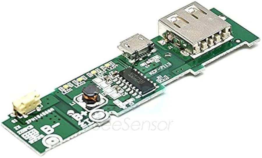
Understanding Mobile Charger PCBs: The Foundation of Your Power Supply
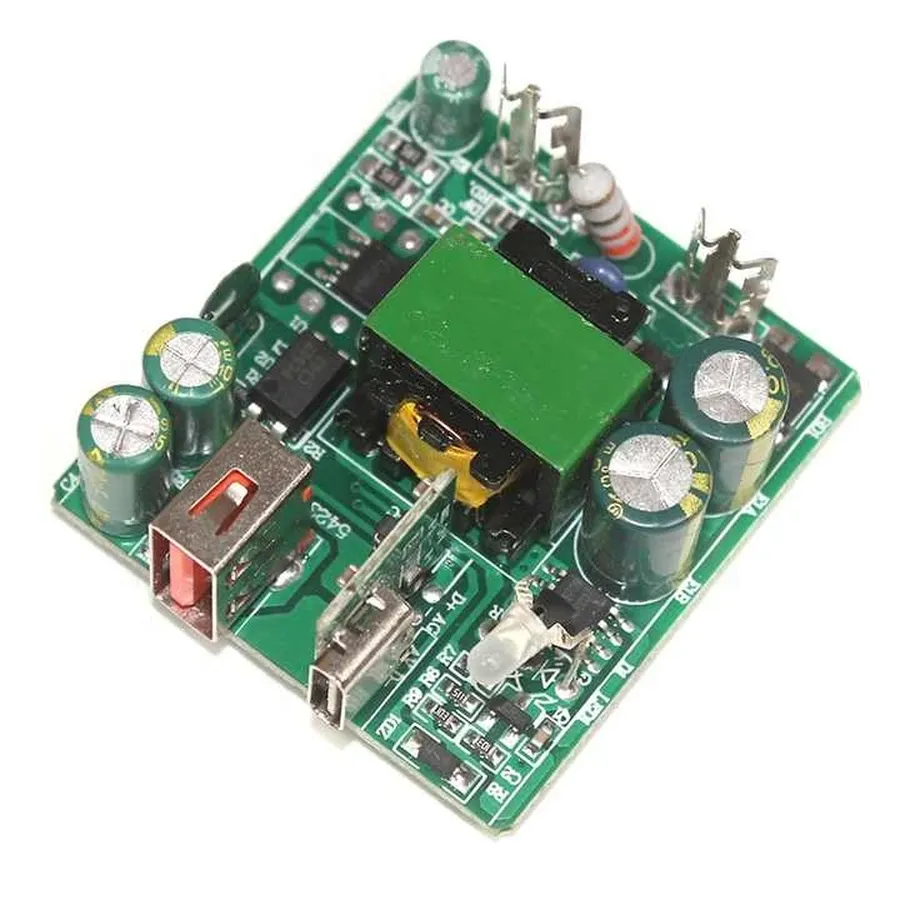
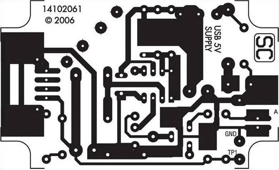
Mobile charger Printed Circuit Boards (PCBs) are the fundamental building blocks of any power adapter for mobile devices, serving as the electrical and mechanical backbone that facilitates power conversion and delivery. These PCBs house the electronic components responsible for transforming mains AC power into the low-voltage DC power needed by smartphones, tablets, and other portable devices. The choice of PCB type and materials significantly impacts the charger's efficiency, reliability, and safety, highlighting the critical role of a mobile charger PCB manufacturer in ensuring high-quality power supplies.
Mobile charger PCBs come in various forms, primarily distinguished by the number of conductive layers they possess. Single-layer PCBs, characterized by their simplicity and cost-effectiveness, are typically found in basic, low-power chargers. Double-layer PCBs, featuring conductive traces on both sides of the substrate, offer increased routing complexity and component density, catering to more sophisticated charging applications. Multi-layer PCBs, composed of three or more conductive layers, are employed in high-performance chargers requiring complex circuitry, improved signal integrity, and enhanced thermal management. Each type of PCB has specific applications, performance characteristics and associated costs that must be considered when choosing the correct board for a design.
The selection of materials for mobile charger PCBs also plays a vital role. The substrate material, typically FR-4, is a composite material known for its electrical insulation properties, mechanical strength, and relative low cost. The copper used for conductive traces determines current-carrying capacity and signal integrity, and the materials used for surface finish affects conductivity, solderability, and corrosion resistance. The expertise of a mobile charger PCB manufacturer is crucial in selecting the most appropriate materials to meet the required performance and durability standards, all while working within the project budget.
Key Factors to Consider When Choosing a Mobile Charger PCB Manufacturer
Selecting the right mobile charger PCB manufacturer is crucial for ensuring the quality and reliability of your final product. This decision impacts everything from production timelines to product performance. Careful evaluation of a manufacturer's capabilities, certifications, and communication processes is essential to a successful partnership.
| Factor | Description | Importance |
|---|---|---|
| Manufacturing Capacity | The volume of PCBs a manufacturer can produce within a given timeframe. | Ensures the manufacturer can meet your current and future demand. |
| Quality Certifications (ISO, UL) | Standardized certifications indicating adherence to quality management systems. | Proof of a manufacturer's commitment to quality and adherence to industry standards. |
| Lead Times | The time required to manufacture and deliver PCBs. | Critical for project timelines and market entry strategies. |
| Minimum Order Quantity (MOQ) | The smallest number of PCBs a manufacturer is willing to produce for an order. | Important to align with your initial production volume requirements. |
| Communication Protocols | The manufacturer's responsiveness and clarity in communication. | Vital for addressing issues quickly and fostering a smooth manufacturing process. |
| Proven Track Record | The manufacturer's history of successfully producing reliable PCBs. | Reduces the risk of selecting an unreliable vendor and ensures product quality |
Types of Mobile Charger PCBs: A Detailed Comparison

Mobile charger PCBs are not monolithic; they come in various configurations, each offering a unique balance of cost, performance, and complexity. The selection of the appropriate PCB type is crucial to the overall performance and reliability of the charger. This section provides a detailed comparison of single-sided, double-sided, and multilayer PCBs, exploring their respective advantages, disadvantages, and typical material usage.
| PCB Type | Complexity | Cost | Performance | Typical Applications | Advantages | Disadvantages |
|---|---|---|---|---|---|---|
| Single-Sided PCB | Low | Lowest | Basic | Simple chargers, low-power applications | Low cost, easy to manufacture | Limited routing, less compact |
| Double-Sided PCB | Medium | Medium | Moderate | Standard chargers, mid-power applications | Increased routing flexibility, better component density | More complex than single-sided, higher cost |
| Multilayer PCB | High | High | High | Advanced chargers, high-power applications, fast charging | High density, best performance, advanced routing capabilities | Highest cost, complex manufacturing process |
Material selection significantly impacts the performance and durability of the PCB. Common materials include FR-4 (a glass-reinforced epoxy laminate), which is widely used due to its balance of cost and performance, and materials with improved thermal properties for high-power applications. The specific material used should be selected based on the power requirements and environmental operating conditions of the charger.
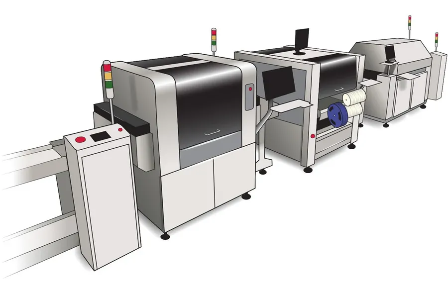
Quality Control in Mobile Charger PCB Manufacturing: Ensuring Reliability and Safety
Rigorous quality control is paramount in mobile charger PCB manufacturing to guarantee the reliability and safety of the final product. A reputable manufacturer implements a series of checks and tests throughout the production process, adhering to industry standards to minimize defects and ensure consistent performance. These quality control measures are not just about meeting specifications; they are critical for preventing failures that could lead to safety hazards or device malfunctions.
| Quality Control Stage | Description | Purpose |
|---|---|---|
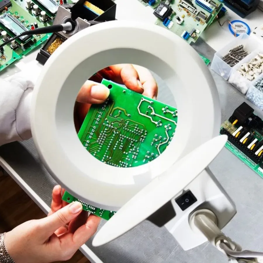
| Visual Inspection | Manual or automated inspection of the bare PCB for surface defects, misalignments, and other visible imperfections. | Identifies manufacturing flaws such as shorts, opens, and improper drilling that may affect functionality. |
| Automated Optical Inspection (AOI) | Automated process that uses high-resolution cameras to capture images of the PCB and compare it to a 'golden board' design to verify correct component placement, solder joints, and other features. | Provides high-speed, consistent detection of defects and ensures the integrity of the assembly process |
| Electrical Testing | Involves various tests such as continuity tests, insulation tests, and functional tests to verify electrical properties of the PCB. | Ensures the PCB meets required electrical performance specifications and identifies potential short circuits, opens, or other connectivity issues. |
| In-Circuit Testing (ICT) | An automated test that checks each component's performance, solder joints, and overall circuitry, simulating the actual operating environment of the circuit. | Checks for correct value and orientation of components, as well as connection integrity after soldering, before power up. |
| Functional Testing | Final test using actual operating conditions to check the overall performance of the circuit board. | Simulates the real-world usage scenarios and ensures the PCB functions as intended within its design specifications. |
| Adherence to IPC Standards | Following the quality and reliability standards set by the IPC (Association Connecting Electronics Industries). | Ensures consistency in manufacturing processes and establishes criteria for acceptable levels of quality. |
Cost Analysis: Factors Influencing the Price of Mobile Charger PCBs

The cost of a mobile charger PCB is determined by a combination of factors, each contributing to the final price. Understanding these drivers allows for more informed decisions when selecting a mobile charger PCB manufacturer and negotiating costs, it's a balance between cost and quality that needs to be carefully considered to optimize the final product.
| Cost Factor | Description | Impact on Price |
|---|---|---|
| Material Costs | The type of substrate material (e.g., FR-4, CEM-1), copper thickness, and solder mask all contribute to the overall material expenses. | Higher-grade materials and thicker copper layers typically increase costs. |
| Manufacturing Complexity | Factors such as the number of layers, the density of components, the complexity of trace routing, via size and count, and the use of blind/buried vias impact the intricacy of the manufacturing process. | Increased complexity generally leads to higher manufacturing costs due to additional processing steps and precision requirements. |
| Order Volume | The quantity of PCBs ordered significantly affects per-unit costs. Larger production runs often benefit from economies of scale. | Larger order volumes usually result in lower per-unit costs due to fixed manufacturing costs being distributed across more units. |
| Surface Finishing | The type of surface finish applied (e.g., HASL, ENIG, Immersion Tin) affects both the performance and cost of the PCB. | Advanced finishes such as ENIG are generally more expensive than HASL but offer superior performance and reliability. |
| Testing Requirements | The extent of electrical testing required (e.g., flying probe test, in-circuit test) impacts cost. | More rigorous and comprehensive testing protocols increase manufacturing costs but ensure higher product reliability. |
| Lead Time | The urgency of delivery can affect cost, with expedited production typically incurring a premium. | Shorter lead times often increase production costs as manufacturers prioritize specific orders. |
Mobile Charger PCB Design Considerations: Optimizing Performance
Efficient PCB design is paramount for optimal mobile charger performance, directly impacting energy conversion, heat management, and overall reliability. A well-designed PCB minimizes power loss, reduces heat generation, and ensures electromagnetic compatibility, all crucial for the safe and efficient operation of mobile chargers. The expertise of a professional design team at the mobile charger PCB manufacturer is essential to achieving these performance goals.
- Trace Width and Impedance Control
Proper trace width is essential for handling the current requirements of the charger without excessive heat buildup. Impedance matching ensures efficient power transfer and minimizes signal reflection. A skilled PCB design team will carefully calculate trace width based on current carrying capacity and the material characteristics and then maintain the correct impedance. - Thermal Management
Mobile chargers generate heat during operation, and effective thermal management is crucial to prevent overheating and premature component failure. This involves careful component placement, the use of thermal vias, and potentially heat sinks to dissipate heat effectively. The PCB design must consider the thermal behavior of all components. - Component Placement
Strategic component placement minimizes signal path lengths, reduces interference, and enhances thermal dissipation. Proper component grouping also minimizes the risk of cross-talk and facilitates efficient circuit operation. A methodical approach is vital for optimal performance. Close attention must be paid to components with high heat dissipation requirements. - Electromagnetic Compatibility (EMC)
EMC considerations are vital to prevent electromagnetic interference (EMI) from affecting nearby electronic devices and ensure that the charger itself is immune to external interference. Shielding, proper grounding techniques, and decoupling capacitors are used. This will also ensure the charger meets all the applicable regulatory requirements. - Layer Stack-up
The arrangement of copper and dielectric layers is important for signal integrity, impedance control, and overall circuit performance. A well-considered stack-up design will help to ensure that signal return paths are effective, power planes are stable and that cross-talk between layers is minimal.
Frequently Asked Questions About Mobile Charger PCBs
This section addresses common queries regarding mobile charger PCBs, focusing on aspects relevant to selecting a manufacturer, understanding PCB types and materials, quality control, and design considerations. These questions are crucial for ensuring you make informed decisions in your product development process.
- What is the typical lifespan of a mobile charger PCB?
The lifespan of a mobile charger PCB is influenced by several factors, including the quality of materials used, the operating environment (temperature, humidity), and the electrical load it experiences. Generally, a well-manufactured PCB can last for several years, often matching or exceeding the expected lifespan of the device itself. However, repeated exposure to high temperatures or excessive current can degrade the PCB over time. A high-quality mobile charger pcb manufacturer uses robust materials and conducts thorough testing, including accelerated life testing, to ensure the PCB meets the required durability standards. Therefore the lifespan of the PCB is not a fixed number, but rather is a function of material selection, manufacturing process and usage. - What certifications should a mobile charger PCB manufacturer possess?
A reputable mobile charger PCB manufacturer should possess several key certifications, most notably ISO 9001 for quality management systems and relevant UL certifications for product safety, which indicates that the manufacturer’s processes and products meet recognized safety standards. Other relevant certifications may include ISO 14001 for environmental management, and specific certifications based on industry or region, such as RoHS for restriction of hazardous substances. These certifications demonstrate a commitment to producing high-quality and safe products and adhering to international industry best practices, thus mitigating the risk of product failure and ensuring compliance with regulations. Thorough due diligence of the manufacturer's certifications should be an essential part of the sourcing process, as these act as third-party validation of their internal quality control processes. - What are the most common issues that affect mobile charger PCBs?
Common issues affecting mobile charger PCBs include trace corrosion due to humidity exposure, solder joint failures due to thermal stress from temperature cycling, and component failures due to overcurrent or overheating. Additionally, design flaws, such as insufficient trace width for high currents, can lead to performance degradation or even safety issues. Insufficient thermal management can also lead to hot spots on the PCB, affecting the lifetime and reliability of the charger. A competent mobile charger pcb manufacturer mitigates these issues through rigorous testing and robust material selection, thus ensuring that the manufactured PCBs meet the performance, durability, and safety requirements set by their customer. Therefore, a strong partnership with a competent manufacturer is essential to mitigate these risks. - How does the type of PCB (single-sided, double-sided, multi-layer) affect charger performance?
The type of PCB significantly impacts charger performance in terms of complexity, cost, and capabilities. Single-sided PCBs are the simplest and most cost-effective but are limited in the complexity of the circuitry they can accommodate. Double-sided PCBs, with conductive layers on both sides, allow for more complex designs with better signal routing but at an increased cost. Multi-layer PCBs, with multiple layers of conductive material, offer the highest complexity and performance, allowing for highly integrated and compact designs with superior signal routing and thermal management but also at the highest cost. The choice of PCB type should be based on the specific requirements of the charger, balancing performance, complexity, and cost, thus ensuring that the optimal balance between performance and cost is achieved. - What materials are commonly used in mobile charger PCBs, and why are they important?
Common materials used in mobile charger PCBs include FR-4 (Flame Retardant type 4), which is a fiberglass-reinforced epoxy laminate due to its cost-effectiveness, mechanical strength, and flame retardancy. High-frequency applications may use materials like Rogers or Teflon for their superior electrical performance, particularly low dielectric loss and low loss tangents, which is essential for high-frequency signals. The selection of PCB materials is crucial as it directly affects the electrical performance, thermal properties, and reliability of the board, ensuring that the PCB functions optimally within its intended operating conditions. A competent mobile charger pcb manufacturer will select the most suitable material that ensures that the PCB will perform to the highest levels within its operational specifications. Therefore, selecting the correct PCB material is critical to both quality and performance. - What quality control measures should I expect from a mobile charger PCB manufacturer?
A reputable mobile charger PCB manufacturer should implement rigorous quality control measures, including Automated Optical Inspection (AOI) for verifying the integrity of the manufactured PCBs, in-circuit testing (ICT) to ensure proper electrical functionality of the assembled components, and X-ray inspection to detect any hidden defects or solder joint issues. Adherence to IPC (Association Connecting Electronics Industries) standards is critical to ensure the reliability of the boards. These quality control measures are crucial for identifying and rectifying defects early in the manufacturing process, therefore reducing the risk of field failures and ensuring that only high-quality boards are delivered. These processes are essential to guarantee consistency and reliability. - How does PCB design affect the thermal management of a mobile charger?
Efficient PCB design plays a crucial role in thermal management in a mobile charger. Proper trace width and copper pour design is essential for effective heat dissipation away from heat-generating components. Good thermal design practices include using thermal vias to conduct heat away from hot spots, and placing components in a way to maximize airflow and heat dissipation from the board to the ambient air. By optimizing PCB layout and trace designs, a mobile charger pcb manufacturer can ensure that the charger can operate effectively without overheating. This is essential to guarantee both high-efficiency and reliability for the end product.
The Future of Mobile Charger PCBs: Innovations and Trends
The mobile charger PCB landscape is undergoing rapid evolution, driven by advancements in materials, manufacturing processes, and consumer demands for more efficient and versatile charging solutions. These trends are reshaping how mobile charger PCB manufacturers operate and innovate, emphasizing the importance of staying at the forefront of technology.
- Integration of Wireless Charging Technology
The demand for wireless charging capabilities is significantly influencing PCB design and manufacturing. Future PCBs will need to incorporate features that support various wireless charging standards, such as Qi, requiring precise antenna designs and advanced power management circuits. This shift also entails the adoption of new materials with suitable magnetic and electrical properties to maximize energy transfer efficiency while minimizing interference. - Flexible PCBs (FPC) for Innovative Charger Designs
Flexible PCBs are gaining traction in mobile charger applications due to their ability to conform to complex and compact form factors. These PCBs facilitate the design of smaller and more versatile chargers, enabling integration into wearable devices and other non-traditional applications. This trend requires manufacturers to invest in advanced fabrication techniques, such as micro-via drilling and specialized lamination processes. - Advancements in Materials for Enhanced Performance
Ongoing research and development are yielding new materials with improved thermal conductivity, electrical properties, and mechanical flexibility. These materials will enable the design of PCBs that are more efficient, durable, and resistant to extreme environmental conditions. The adoption of materials like advanced ceramics, high-performance polymers, and graphene composites is expected to enhance the performance and longevity of mobile chargers. - Miniaturization and High-Density Interconnect (HDI) PCBs
The trend toward smaller, more powerful devices demands miniaturized PCB designs with increased circuit density. High-Density Interconnect (HDI) technology will become increasingly essential for manufacturing mobile charger PCBs that can support complex functionalities in constrained spaces. This includes the use of smaller vias, finer trace widths, and advanced surface finish technologies. - Sustainable and Environmentally Friendly Manufacturing
The industry is increasingly focusing on sustainable manufacturing practices. This includes the use of eco-friendly materials, reduction of waste, and adoption of energy-efficient production processes. PCB manufacturers are actively seeking solutions that minimize their environmental footprint, driving innovation in both materials and manufacturing technologies. This shift requires manufacturers to invest in recycling programs and implement stricter environmental protocols.
Finding the Right Mobile Charger PCB Manufacturer: A Practical Guide
Selecting the appropriate mobile charger PCB manufacturer is crucial for ensuring product quality, reliability, and timely delivery. This section provides a structured guide to help you navigate the process of finding, evaluating, and choosing a manufacturer that meets your specific needs, ultimately fostering a successful partnership.
- Define Your Requirements
Begin by clearly outlining your specific needs. This includes the type of PCB (single-layer, double-layer, multi-layer), material requirements (e.g., FR-4, aluminum), performance specifications, required certifications, and any special features. Understanding your exact needs will narrow down the list of potential manufacturers. - Initial Research
Use online resources, such as industry directories, B2B platforms, and search engines, to identify potential manufacturers. Look for companies that specialize in mobile charger PCBs and have relevant experience. Trade shows and industry events are also excellent opportunities to discover manufacturers. - Shortlist Potential Manufacturers
Based on your initial research, compile a shortlist of manufacturers that appear to meet your needs. Consider factors like location, manufacturing capacity, and areas of specialization. A balanced consideration of these factors is critical to prevent supply chain and lead time challenges. - Evaluate Capabilities
Assess each manufacturer's capabilities by reviewing their website, requesting company profiles, and engaging in discussions. Look for evidence of quality certifications (ISO, UL, etc.), advanced manufacturing equipment, robust quality control processes, and a skilled design and engineering team. - Request Quotes and Samples
Once you have a shortlist, request detailed quotes for your project. Specify your PCB requirements and ask for sample PCBs for testing and evaluation. This provides a tangible way to assess quality, performance, and adherence to specifications. - Evaluate Samples and Conduct Testing
Thoroughly inspect the sample PCBs and conduct necessary tests to verify that they meet your requirements, including electrical testing, performance checks, and durability assessments. Evaluate the testing process performed by the manufacture as well. - Assess Communication and Support
Good communication and responsiveness are essential for a successful partnership. Evaluate how well the manufacturer communicates, how quickly they respond to inquiries, and their ability to provide technical support. A strong support system is necessary for seamless collaboration. - Negotiate Terms and Conditions
Once you have made your choice, negotiate terms and conditions with your preferred manufacturer, including pricing, delivery schedules, payment terms, and warranty. Ensuring all terms are clearly agreed upon upfront minimizes potential misunderstandings and conflicts. - Establish a Long-Term Partnership
Consider the potential for a long-term partnership. A reliable and trusted manufacturer can simplify your supply chain and provide consistently high-quality products. Building long-term relationships can improve product quality, reduce costs, and enhance overall reliability.
Selecting the right mobile charger PCB manufacturer is a crucial decision that impacts the performance, reliability, and safety of your products. By thoroughly understanding the technical considerations, quality control measures, and cost factors outlined in this guide, you're better equipped to make an informed decision. Remember that a partnership with a dependable mobile charger pcb manufacturer ensures you can stay ahead of the curve in the rapidly evolving landscape of mobile technology. Continuous learning, exploration of new technologies, and an emphasis on innovation are vital to staying relevant in this dynamic sector.