Selecting a Reliable 10 Layer PCB Manufacturer: A Comprehensive Guide
In today's rapidly evolving electronics landscape, multilayer PCBs have become indispensable, with 10 layer PCBs finding their way into sophisticated applications, from advanced medical devices to complex industrial control systems and cutting-edge telecommunications equipment. Selecting a trustworthy 10 layer pcb manufacturer is not just a matter of choosing a supplier; it is a strategic decision that directly impacts the quality, reliability, and overall success of your electronic products. This article explores the intricacies of selecting the right manufacturing partner, helping you understand the key factors and make informed choices.
Understanding 10 Layer PCB Technology
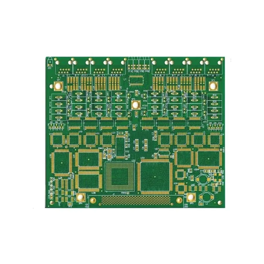
10-layer printed circuit boards (PCBs) represent a significant advancement in electronic design, offering a complex architecture that enables the integration of sophisticated functionalities. These boards consist of ten conductive layers, separated by insulating material, allowing for a higher density of interconnections, improved signal integrity, and enhanced power distribution compared to single- or double-sided PCBs. This section delves into the nuances of 10-layer PCB technology, covering the benefits, stack-up configurations, and material selection.
The primary advantage of using 10-layer PCBs is their capacity to handle complex routing challenges, which is critical for high-density circuits. By having multiple layers, designers can efficiently manage the routing of numerous signal traces, often separating sensitive analog and high-speed digital signals. This layer separation helps reduce interference and improve overall signal quality, which is essential for reliable electronic operation. The multiple layers also allow for dedicated power and ground planes, reducing impedance, improving power distribution, and minimizing noise. This careful layer management leads to a more stable, reliable, and high-performance electronic device.
| Feature | Single/Double-Sided PCB | 10-Layer PCB |
|---|---|---|
| Routing Complexity | Limited | High |
| Signal Integrity | Lower | Higher |
| Power Distribution | Basic | Advanced |
| Layer Count | 1-2 | 10 |
| Design Flexibility | Low | High |
| Cost | Lower | Higher |
Stack-up configurations in 10-layer PCBs typically involve alternating signal, power, and ground layers. The exact arrangement can vary based on application requirements. A common configuration might include two outer signal layers, followed by a ground plane, a power plane, and several internal signal layers, along with additional power and ground layers. This stack-up design ensures optimal impedance control, noise reduction, and efficient power distribution. Material choices for 10-layer PCBs play a significant role in their performance; typically, FR-4 is used, with options for higher-performance materials for specific applications. Understanding the impact of the different stackup and material options will impact your choice of 10 layer PCB manufacturer.
Key Considerations When Choosing a 10 Layer PCB Manufacturer
Selecting the right 10-layer PCB manufacturer requires a thorough evaluation of their capabilities and quality standards. The ideal manufacturer must reliably produce complex boards to meet the specific demands of advanced electronic designs. This section details the key factors to consider when making this crucial decision, ensuring that the chosen partner can consistently meet your project's technical and quality requirements.
- Manufacturing Capabilities
Assess the manufacturer's capacity to handle 10-layer PCBs, including their maximum board size, minimum trace/space width, and via drilling capabilities. Ensure they can meet the specific design requirements of your project. For example, if your design includes very fine-pitch components and high-density routing, verify that the manufacturer can achieve these specifications consistently. - Material Options
Confirm the availability of various materials, such as FR-4, high-Tg FR-4, and specialized laminates, to meet different thermal, electrical, and mechanical requirements. The dielectric properties and thermal performance of the materials used are vital for the final performance of your PCBs. - Surface Finish Options
Evaluate the available surface finish options (e.g., ENIG, HASL, OSP) and their suitability for your specific application, considering factors like solderability and environmental resistance. The selected finish must be appropriate for your assembly and operational environment. - Quality Control Practices
Verify that the manufacturer adheres to rigorous quality control standards and employs appropriate testing methods (e.g., electrical testing, impedance testing, X-ray inspection). This ensures that the PCBs consistently meet the required performance and reliability criteria. - Certifications
Look for manufacturers with certifications like ISO 9001 and other industry-specific standards, as they indicate a commitment to quality management and continuous improvement. These certifications provide a level of assurance regarding the quality management systems in place.
| Factor | Description | Importance |
|---|---|---|
| Layer Count Capacity | The maximum number of layers the manufacturer can reliably produce. | Critical for complex designs requiring multiple signal and power layers. |
| Minimum Trace/Space | The smallest track and gap widths achievable, which impact routing density. | Essential for designs with high-density routing. |
| Material Availability | The variety of laminate materials offered, including FR-4, high-Tg FR-4, and others. | Impacts the thermal and electrical performance of the final product. |
| Surface Finish Options | Different finishes available like ENIG, HASL, and OSP. | Affects solderability, corrosion resistance, and contact reliability. |
| Quality Control | Manufacturing process controls and testing methods to ensure the reliability of boards. | Critical for avoiding defects and ensuring compliance with specifications. |
| Certifications | ISO 9001 or similar certifications for quality management systems. | Indicates commitment to quality management and continuous improvement. |
Comparing Leading 10 Layer PCB Manufacturers
Selecting the right 10-layer PCB manufacturer requires a careful comparison of their capabilities, pricing, and customer service. This section offers a comparative analysis of prominent manufacturers, enabling informed decision-making based on your project's specific demands for cost, speed, and quality.
| Manufacturer | Specialization | Turnaround Time | Pricing | Customer Service | Strengths | Weaknesses |
|---|---|---|---|---|---|---|
| Manufacturer A | Prototyping and small-batch production | 5-10 business days | Moderate to High | Excellent | Fast prototyping, strong communication | Higher prices for large-scale orders |
| Manufacturer B | Mass production | 2-4 weeks | Competitive | Good | Cost-effective for high volumes | Longer lead times for prototypes |
| Manufacturer C | Specialized PCBs (e.g., RF, high-speed) | 10-15 business days | High | Excellent, technically proficient | Expertise in specialized applications | Higher price point and longer lead times |
| Manufacturer D | Hobbyist and small businesses | 7-12 business days | Low to Moderate | Good, responsive | Affordable for small orders | May not have advanced manufacturing for very high-density boards. |
Note: The table above provides a general comparison. Actual performance and capabilities may vary. It is crucial to contact manufacturers directly to receive a custom quote based on your specific design needs.
Material Selection for 10 Layer PCBs
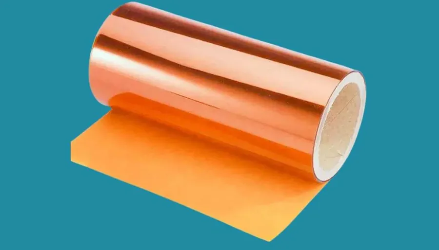
The selection of materials for 10-layer PCBs is critical to their performance and reliability, impacting thermal management, signal integrity, and overall longevity. The appropriate material choice is dictated by the intended application and operating environment, necessitating a thorough evaluation of characteristics such as thermal performance, dielectric constant, and mechanical strength.
| Material Type | Description | Typical Applications | Advantages | Disadvantages |
|---|---|---|---|---|
| FR-4 | The most commonly used material for PCBs, composed of woven fiberglass cloth with epoxy resin. | General purpose applications, consumer electronics, low to mid-frequency circuits. | Cost-effective, widely available, good mechanical strength, suitable for most standard applications. | Lower thermal performance compared to specialized materials, moderate dielectric constant variations with temperature. |
| High-Tg FR-4 | An enhanced version of FR-4 with a higher glass transition temperature (Tg), indicating better temperature resistance. | Applications requiring higher thermal performance, such as automotive, industrial, and power electronics. | Improved thermal stability and performance, greater resilience under high heat conditions, lower warpage. | Higher cost than standard FR-4, may be less readily available. |
| Polyimide | A high-performance material with excellent thermal and electrical properties. | High-frequency applications, aerospace and military applications, circuits with high operating temperatures and demanding thermal conditions. | Exceptional thermal performance, stable dielectric constant across a wide temperature range, excellent flexibility. | Significantly higher cost compared to FR-4 materials, more complex fabrication processes. |
| Rogers Materials | A family of advanced materials with a focus on high-frequency and high-speed applications. | RF and microwave applications, high-speed digital circuits, telecommunications infrastructure. | Superior electrical properties, very low dielectric loss, highly stable performance at high frequencies. | Higher cost and potentially more challenging fabrication than FR-4. |
- Thermal Performance Considerations
The material's thermal conductivity and glass transition temperature (Tg) are vital for ensuring reliable operation. High-Tg materials are often needed to handle high operational temperatures or where there are higher heat dissipation requirements within the PCB, such as within power supplies or high speed circuitry. - Dielectric Constant
The dielectric constant influences signal propagation speed and impedance and is a crucial material characteristic for high speed signal integrity. It is essential to choose a material that provides a stable dielectric constant with minimal variations in temperature and frequency to ensure signal integrity and performance. - Mechanical Strength and Stability
The material needs to have sufficient mechanical strength to withstand the stresses of manufacturing and the rigours of the operating environment, including thermal cycling. Mechanical strength is influenced by the material’s composition and thickness. For example, FR-4 provides good general-purpose mechanical strength, whereas polyimide offers excellent flexibility, this makes it useful for applications needing flexible PCBs. The selected materials must have mechanical stability, allowing for a stable substrate for mounted components. - Cost Implications
Material choices significantly impact the cost of a 10-layer PCB, with advanced materials, such as Rogers or Polyimide, costing significantly more than standard FR-4 or High-Tg FR-4. Balancing performance requirements with cost constraints is a key design consideration. - Material Availability and Supply Chain
Consider the availability of the material in the supply chain. Standard materials like FR-4 have a mature and robust supply chain, whereas some high-performance materials may be more specialized and have a higher lead time associated with them. This will impact the selection process, specifically regarding cost and delivery.
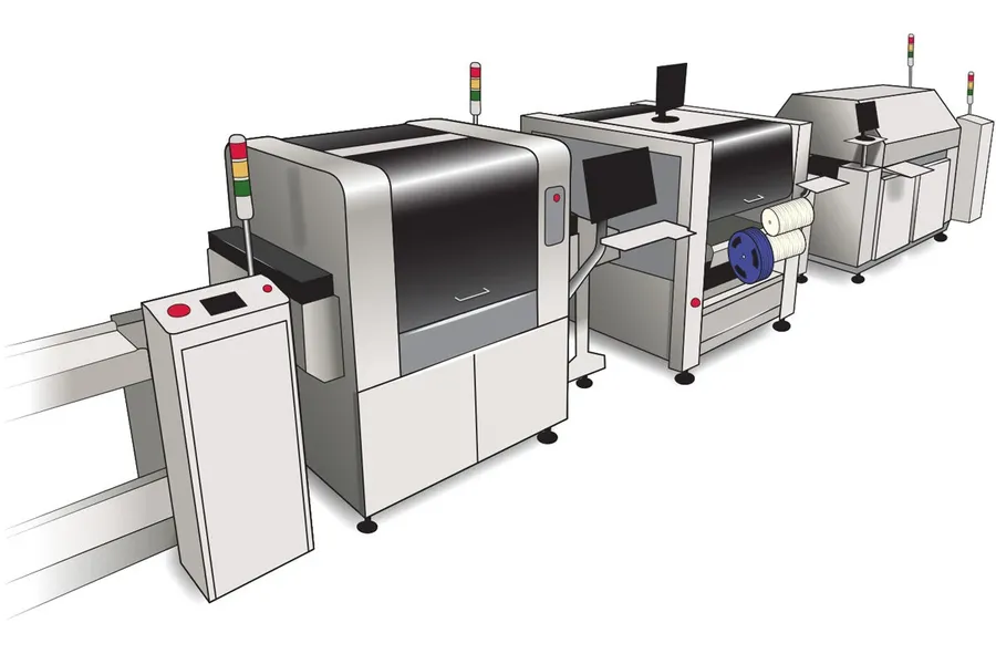
Advanced PCB Design and Manufacturing for 10 Layer Boards
Designing and manufacturing 10-layer PCBs requires meticulous attention to detail, as these boards support complex electronic systems with high-density signal routing, robust power delivery, and thermal management. Optimizing these factors is crucial to achieve reliable and high-performance electronic products. Advanced techniques in both design and manufacturing are essential to realize the full potential of a 10 layer PCB.
- Signal Integrity Considerations
Maintaining signal integrity in a 10-layer PCB is paramount for high-speed data transmission. This involves precise impedance control and trace routing to minimize reflections, signal loss, and crosstalk. Differential pair routing and appropriate trace terminations are frequently used. - Power Distribution Network (PDN)
Effective power distribution is essential for 10 layer PCBs. A well designed PDN includes dedicated power and ground planes, sufficient decoupling capacitors and proper via placement to reduce noise and maintain stable power supply to components. - Thermal Management Techniques
Effective heat dissipation is crucial to maintain operational integrity and longevity. Techniques include using thermal vias to transfer heat away from heat-generating components, incorporating heat sinks, and using materials with high thermal conductivity. Layer stack up design can also optimize heat transfer. - Impedance Control Strategies
Controlling impedance is crucial for signal integrity especially at high frequencies. The dimensions and the dielectric properties of the PCB material along with the trace geometry are all critical factors. The PCB manufacturer must have a high level of expertise and provide consistent output for impedance control.
| Manufacturing Process | Description | Impact on 10 Layer PCBs |
|---|---|---|
| Via Drilling | Creating conductive pathways between different layers. This includes through-hole, blind, and buried vias. | High precision is required for accurate layer connections. Smaller vias increase routing density and enable finer designs. |
| Plating | Applying a conductive metal layer to the surfaces and drilled vias. This process uses copper plating for conductivity and often includes a surface finish for solderability. | Uniform plating is essential for consistent conductivity across all layers. Good via plating quality will ensure strong electrical connections |
| Multilayer Lamination | Bonding multiple layers together using heat and pressure. The layers are stacked with precise alignment. | Precise alignment and uniform pressure are necessary to prevent warping and delamination. This step is critical to ensuring the stability and reliability of a 10 layer PCB. |
| Advanced Etching | Using a chemical process to remove excess copper, leaving the desired traces and patterns on each layer. | High precision etching is necessary to maintain signal integrity with very fine traces and spaces that are often present in multi-layer designs. |
Working closely with a 10-layer PCB manufacturer that has expertise in these advanced design and manufacturing practices is vital for achieving the desired performance. This collaboration ensures that the PCB meets the precise specifications of the project, offering high signal quality, reliable power delivery, and effective thermal management.
Frequently Asked Questions about 10 Layer PCBs
This section addresses common questions regarding 10-layer PCBs, providing clear and concise answers to help you understand their specifications, design considerations, and applications.
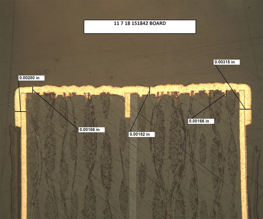
- What is the typical thickness of a 10-layer PCB?
The typical finished thickness of a 10-layer PCB is around 1.6mm (0.063 inches), though this can vary depending on design requirements and specific material choices. The thickness of the core and prepreg materials used in the PCB stack-up are the primary determinants. Manufacturers can adjust these thicknesses based on the project needs. Other thicknesses are also available but may have minimum order quantities or require custom manufacturing. - What design rules should I consider for a 10-layer PCB?
Key design rules for 10-layer PCBs include minimum trace width and spacing, via size and type, impedance control requirements, and layer stack-up configuration. The complexity of a 10-layer PCB demands meticulous planning to ensure signal integrity, power distribution, and thermal management. Following the IPC standards for PCB design is highly advised. - What are the typical cost considerations for 10-layer PCB manufacturing?
The cost of manufacturing 10-layer PCBs is affected by factors such as material costs, board size, complexity, via count, surface finish requirements, and order volume. The choice of material, especially high-performance materials such as high-Tg FR-4, can significantly impact the overall cost. Cost savings can be achieved through design optimization and efficient panelization and also working with a manufacturer that has volume capacity. - Which industries commonly utilize 10-layer PCBs?
10-layer PCBs are commonly found in industries that require high-performance, high-density electronics, including telecommunications, aerospace, medical devices, industrial control, and high-performance computing. These industries often demand the superior signal integrity, power distribution, and routing capabilities that multi-layered boards provide. - How does the board thickness relate to the number of layers in a PCB?
The overall thickness of a PCB is determined by the thickness of individual layers, including the core and prepreg materials, rather than simply the layer count. A 10-layer board is usually thicker than a 4-layer PCB, but it's the material properties of those layers that also contribute to the overall thickness. Thicker PCBs are often preferred for structural rigidity or specific impedance needs, which may also contribute to a higher layer count. - How can I achieve optimal signal integrity in a 10-layer PCB?
Achieving optimal signal integrity involves careful layer stack-up design, controlled impedance routing, proper termination techniques, and good grounding practices. Utilizing power and ground planes can minimize noise, while trace routing should avoid abrupt bends and unnecessary vias, which can cause reflections. Use simulation tools early in the design process to predict and optimize signal integrity performance. - What regulatory standards should I be aware of when designing and manufacturing 10-layer PCBs?
Key regulatory standards for PCB manufacturing include IPC standards such as IPC-A-600 for PCB acceptability, IPC-6012 for performance specifications, and also industry-specific standards, for example ISO 13485 for medical devices. Environmental regulations such as RoHS (Restriction of Hazardous Substances) compliance are also critical. Choosing a manufacturer that adheres to these standards is essential for regulatory compliance and the quality of the PCBs.
Cost Analysis for 10 Layer PCB Manufacturing
Understanding the cost drivers in 10-layer PCB manufacturing is crucial for effective budgeting and cost optimization. This section provides a detailed cost analysis covering key factors that influence pricing, and strategies to manage expenses without compromising performance. By understanding these cost elements, you can make informed decisions when selecting a 10 layer PCB manufacturer.
| Cost Factor | Description | Impact on Cost |
|---|---|---|
| Material Costs | The base material used (e.g., FR-4, high-Tg FR-4) and other materials for lamination and finish | Significant impact, varies with material type and quality |
| Layer Count | Number of conductive layers in the PCB stack-up | Directly proportional to cost, as each layer requires additional processing |
| Board Complexity | Density of traces, vias, pads, and component placement | Higher complexity increases manufacturing time and tooling costs |
| Tooling Charges | Costs for creating necessary tools and patterns for manufacturing | Initial setup costs, can be significant for low-volume orders |
| Order Volume | Quantity of PCBs ordered in a single batch | Higher volume often leads to lower per-unit costs due to economies of scale |
| Surface Finish | Type of finish (e.g., HASL, ENIG, Immersion Tin) | Varies with type; ENIG is usually more costly than HASL |
| Testing and Quality Control | Inspection and testing processes to ensure PCB functionality | Essential for reliability; affects overall manufacturing cost |
| Turnaround Time | Requested time for manufacturing | Faster turnaround times generally incur higher fees |
- Cost Optimization Techniques
Several techniques can be employed to optimize costs in 10-layer PCB manufacturing. These include: * **Design for Manufacturing (DFM):** Optimizing the design to reduce manufacturing complexity, such as using standard via sizes and avoiding unnecessary tight tolerances. * **Panelization:** Ordering multiple PCBs on a single panel to save costs at higher volumes. * **Material Selection:** Choosing cost-effective materials without compromising performance for the application. * **Component Selection:** Choosing more readily available and less expensive components to reduce overall costs. - Budgeting Tips
When budgeting for 10-layer PCB manufacturing, consider including a buffer for unexpected costs. Obtain quotes from multiple manufacturers to compare pricing. Consider costs associated with prototyping and iterative design revisions in order to achieve optimal results from the 10 layer pcb manufacturer.
Future Trends in 10 Layer PCB Technology
The landscape of 10-layer PCB technology is rapidly evolving, driven by miniaturization, the emergence of novel materials, and a growing emphasis on sustainable manufacturing practices. These advancements are not only reshaping PCB design but also expanding the range of applications for these complex circuit boards. Understanding these trends is crucial for any organization selecting a 10-layer PCB manufacturer, as these trends will impact material availability and design specifications.
- Miniaturization
The ongoing push towards smaller and more compact electronic devices is driving the need for higher-density PCBs. This translates into finer lines and spacing, smaller vias, and more advanced techniques for component placement and routing on 10-layer boards. This impacts the complexity of design and the manufacturing capabilities of 10-layer PCB manufacturers. - Advanced Materials
Traditional FR-4 materials are gradually being supplemented by new materials with enhanced thermal performance, improved dielectric properties, and greater mechanical strength. These advanced materials often include high-Tg FR-4, ceramics, and composites, catering to the demanding requirements of high-speed and high-temperature applications. Material selection is now as crucial as manufacturer selection. - Sustainable Manufacturing
The environmental impact of PCB manufacturing is receiving increased scrutiny. The industry is exploring sustainable solutions such as the use of eco-friendly materials, reduced waste production, and more energy-efficient manufacturing processes. Selecting a manufacturer that prioritizes these sustainable practices will be essential for business that aim to reduce their environmental impact. - Integration of Embedded Components
Embedding components directly within the PCB layers is becoming more common in advanced designs for 10-layer PCBs. This technique reduces board size, improves signal integrity, and allows for more efficient designs. Selecting a manufacturer capable of this will be essential for some advanced applications. - Advanced Design Simulation Tools
The increase of complexity in the design process means the use of advanced simulation tools are necessary to accurately predict performance. These tools enable the optimization of layer stack-ups, signal routing, and thermal management before production, which greatly improves efficiency.
Actionable Steps for Selecting Your 10 Layer PCB Manufacturer
Selecting the right 10-layer PCB manufacturer is crucial for ensuring the success of your electronic product. This section provides a structured approach to effectively vet potential manufacturing partners, ensuring a robust, reliable, and cost-effective production process. Prioritizing a manufacturer that can act as a long-term business partner is critical for consistent quality and support.
- Prepare a Detailed Request for Quotation (RFQ)
Your RFQ should be comprehensive, including precise design specifications, desired materials (e.g., FR-4, high-Tg FR-4), specific layer stack-up requirements, required surface finish (e.g., ENIG, HASL), expected production volume, and desired delivery timeline. Be very clear about your tolerances and performance criteria. - Assess Manufacturing Capabilities
Verify that the manufacturer possesses the necessary equipment and expertise to handle 10-layer PCB fabrication. Confirm their capability to meet required trace widths and spacing, via drilling techniques, impedance control, and multilayer lamination processes. Request examples or case studies of their past 10-layer PCB production. - Evaluate Quality Control and Certifications
Ensure the manufacturer adheres to industry-standard quality management practices. Check for certifications such as ISO 9001, ISO 13485 (for medical devices), or IATF 16949 (for automotive). Inquire about their quality control processes, including in-process inspections and final product testing procedures to guarantee high reliability. - Request and Analyze Prototype PCBs
Before committing to full-scale production, request a prototype run. This allows you to thoroughly evaluate the PCBs, check for any fabrication or design issues, and confirm that the manufacturer's results align with your specifications. It's also vital to test the prototype under simulated operating conditions to verify thermal performance. - Investigate Turnaround Time and Pricing
Evaluate the manufacturer's ability to meet your required delivery timelines, considering both prototype and mass production needs. Obtain detailed cost estimates for the PCB production, including any potential tooling or setup costs. Assess the overall value proposition and not just price alone, weighing speed of production and quality with cost. - Verify Communication and Support
Assess the responsiveness and helpfulness of the manufacturer's communication channels. A good manufacturer should be readily available to address technical queries and provide assistance as needed. Test how well they can resolve issues during the prototype phase and establish clear communication channels. - Establish a Long-Term Partnership
Consider a manufacturer that values long-term partnership. Discuss your ongoing production needs and future projects, ensuring they have the capacity and commitment to support your long-term requirements. A long term business relationship will allow for continuous improvements in manufacturing and pricing.
Choosing the right 10 layer pcb manufacturer is a critical decision that affects the entire lifecycle of your product, from design to final assembly. By carefully considering the factors outlined in this article—from technical specifications to manufacturing capabilities and future trends—you can select a manufacturer that aligns perfectly with your project goals, budget, and timeline. Remember, partnering with a reliable 10 layer pcb manufacturer ensures that your PCBs will perform to the standards required for your application, contributing directly to your product’s overall success. Evaluate your needs against manufacturer capabilities and ensure they have proven experience in producing similar complex PCBs.