Top Printed Wiring Board Manufacturers: A Comprehensive Guide
Printed wiring boards (PWBs), the backbone of modern electronics, are ubiquitous, from our smartphones to complex industrial machinery. Choosing the right printed wiring board manufacturers is crucial for product reliability and performance. This article delves into the landscape of top PWB manufacturers, their capabilities, and key factors in selection, ensuring your electronic projects get the best foundation.
Understanding the Role of Printed Wiring Board Manufacturers
Printed Wiring Board (PWB) manufacturers are the cornerstone of the modern electronics industry, transforming intricate designs into the physical platforms upon which electronic components are mounted and interconnected. Their role extends from interpreting complex circuit schematics to fabricating and assembling the boards with high precision and reliability, ultimately determining the quality and functionality of electronic devices.
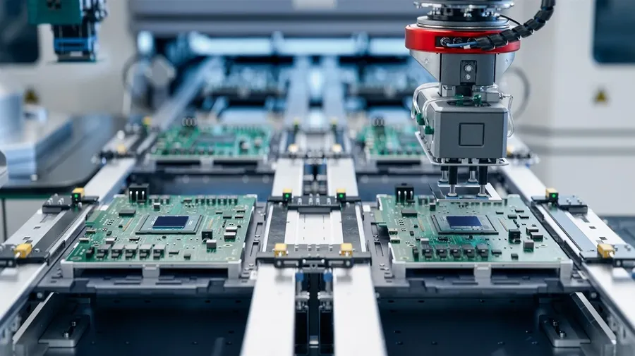
These manufacturers are not simply fabricators; they are critical partners in the product development cycle. They collaborate closely with design engineers, offering design for manufacturability (DFM) feedback, ensuring designs can be reliably and cost-effectively produced. The manufacturing process involves several key stages, each with specific quality and precision requirements: material selection, circuit pattern creation, etching, drilling, plating, solder mask application, component assembly and rigorous testing.
The proficiency of PWB manufacturers directly influences the performance and lifespan of electronic products. From simple single-sided boards to complex multi-layered structures with advanced materials, the capability of these manufacturers impacts the density, reliability, and functionality of various electronic applications, ranging from consumer electronics to aerospace and medical devices. They contribute to product quality not just in terms of fabrication precision, but also through their adherence to strict industry standards and quality control protocols. This critical role makes their selection a crucial decision in product development.
Key Capabilities to Look for in PWB Manufacturers

Selecting the right Printed Wiring Board (PWB) manufacturer is crucial for ensuring the quality and reliability of electronic products. This section outlines essential capabilities that should be considered when evaluating potential PWB manufacturing partners, focusing on fabrication technology, assembly services, certifications, prototyping options, turnaround times, and quality control.
| Capability | Description | Importance |
|---|---|---|
| Fabrication Technology | Capabilities in handling various materials (e.g., FR-4, polyimide), layer counts, and trace widths, as well as advanced technologies like HDI and flex PCBs. | Directly affects the complexity and performance of the final product. A manufacturer with advanced tech can meet more varied needs. |
| Assembly Services | Offers SMT, through-hole, and mixed technology assembly; in-house capabilities or partnerships for efficient component placement. | Ensures seamless production from bare board to populated PCB, saving time and reducing risk of errors from multiple vendors. |
| Certifications (AS9100D, ISO) | Complies with industry standards like AS9100D for aerospace/defense or ISO 9001 for general quality management; shows commitment to quality and reliability. | Provides assurance of consistent quality, especially important for high-reliability applications. |
| Prototyping Options | Offers rapid prototyping for quick testing and design iterations; ability to scale up from prototypes to large production volumes. | Allows for early validation of designs and reduces the time and cost of getting a product to market. |
| Turnaround Time | Delivers products on time with flexible options based on project urgency; capability to expedite production for urgent needs. | Is critical for time-sensitive projects; shorter lead times reduce time-to-market. |
| Quality Control | Rigorous testing and inspection processes at every production stage; uses automated optical inspection (AOI) and electrical testing. | Ensures the reliability and performance of the finished product; reduces the risk of field failures. |
Top Printed Wiring Board Manufacturers in the USA

The United States is home to numerous high-quality printed wiring board (PWB) manufacturers, each with unique specializations and strengths. These manufacturers cater to a wide range of industries, from aerospace and defense to medical and consumer electronics, offering diverse production capabilities, from rapid prototyping to high-volume manufacturing.
The PWB manufacturing landscape in the USA is characterized by a blend of established players and innovative newcomers. This section highlights several leading manufacturers, focusing on their key capabilities, technological strengths, and areas of specialization. Understanding these distinctions can help in selecting the most appropriate partner for specific project needs.
| Manufacturer | Specialization | Key Strengths | Production Volume |
|---|---|---|---|
| Company A | Aerospace and Defense | High-reliability PWBs, AS9100D certification, advanced materials | Low to Medium |
| Company B | Medical Devices | Rigid-flex PCBs, biocompatible materials, ISO 13485 certification | Medium to High |
| Company C | Industrial Automation | Heavy copper PCBs, robust designs, UL certification | Medium to High |
| Company D | Consumer Electronics | High-density interconnect (HDI) PCBs, SMT assembly, quick turnaround | High |
| Company E | Telecommunications | High-speed PCBs, impedance control, RF and microwave capabilities | Low to Medium |
The table above highlights a small subset of the leading PWB manufacturers in the USA. When choosing a PWB manufacturer, it is vital to consider whether the manufacturer specializes in low, medium, or high volume production, as this will greatly impact delivery times and cost. Some manufacturers focus on rapid prototyping and quick turnarounds while others are optimized for large-scale production.
Global Leaders in Printed Wiring Board Manufacturing

The global printed wiring board (PWB) manufacturing landscape is characterized by a mix of established giants and emerging players, each contributing to technological innovation and market dynamics. International manufacturing is primarily driven by cost optimization, specialized capabilities, and strategic market positioning, impacting the availability and pricing of PWBs worldwide.
Key factors influencing international PWB manufacturing include:
- Cost Efficiency
Countries with lower labor costs and favorable economic policies often attract large-scale PWB production, allowing manufacturers to offer competitive prices. - Technological Expertise
Certain regions excel in specific PWB technologies, such as high-density interconnect (HDI), flexible PCBs, or advanced materials, which makes them preferred partners for particular applications. - Supply Chain and Logistics
Proximity to major electronics manufacturing hubs and efficient logistics networks play a critical role in ensuring timely delivery and reduced shipping costs, influencing the choice of manufacturing location. - Government Policies and Trade Agreements
Government incentives, tax benefits, and trade agreements can significantly affect the competitiveness and attractiveness of certain regions for PWB manufacturing.
The impact of global manufacturing on the PWB industry is multifaceted:
- Cost
Offshore manufacturing, particularly in Asia, often leads to lower production costs, translating to lower prices for consumers. - Availability
Global production networks increase the supply of PWBs, catering to diverse needs and enabling businesses to source components efficiently. - Innovation
Competition among international manufacturers fosters innovation in materials, processes, and manufacturing technologies, pushing the boundaries of PCB design and performance.
Specialized PCB Services: Beyond Standard Manufacturing

Beyond standard printed circuit board manufacturing, a range of specialized services are offered by leading manufacturers to meet the diverse needs of the electronics industry. These advanced services encompass technologies like High Density Interconnect (HDI), flexible PCBs, Surface Mount Technology (SMT), and rigorous testing procedures, catering to complex and demanding applications.
| Service | Description | Typical Applications |
|---|---|---|
| High Density Interconnect (HDI) PCBs | PCBs with higher wiring density per unit area achieved through microvias and fine lines. | Smartphones, wearable electronics, high-performance computing. |
| Flexible PCBs (Flex PCBs) | PCBs built on flexible substrates, allowing for bending, twisting, and shaping. | Aerospace, automotive, medical devices, wearable technology. |
| Surface Mount Technology (SMT) | Automated assembly of electronic components directly onto the surface of a PCB, enabling higher circuit density. | Consumer electronics, automotive electronics, industrial control systems. |
| Comprehensive Testing | Rigorous electrical and functional testing to verify the integrity and performance of PCBs including In-Circuit Testing (ICT), Flying Probe Testing, Automated Optical Inspection (AOI). | All electronics requiring high reliability and performance. |
Choosing the Right Printed Wiring Board Manufacturer: A Step-by-Step Guide

Selecting the appropriate printed wiring board (PWB) manufacturer is a critical decision that directly impacts the quality, cost, and delivery timeline of your electronic product. A systematic approach is essential to ensure your chosen manufacturer aligns with your project's specific requirements and overall objectives.
- Define Project Requirements
Begin by clearly defining your project's specific requirements. This includes the type of PCB (single-layer, multi-layer, flexible, rigid-flex), the dimensions, layer count, materials (FR-4, aluminum, polyimide), required impedance control, surface finish (ENIG, HASL), and any special performance or environmental considerations. - Assess Manufacturing Capabilities
Evaluate potential manufacturers based on their fabrication capabilities. Confirm they possess the necessary technology and equipment to meet your PCB design specifications, including minimum trace width, spacing, hole size, and layer stack-up capabilities. Ensure the manufacturer can support your required production volume and time frame. - Verify Certifications and Quality Standards
Confirm that the manufacturer adheres to industry-recognized quality standards and holds relevant certifications such as ISO 9001, AS9100D (for aerospace), or ISO 13485 (for medical devices). These certifications are indicators of rigorous quality control processes, traceability, and process consistency. - Evaluate Prototyping and Turnaround Time
Consider the manufacturer's capability for rapid prototyping. Quick turnaround times for initial prototypes and revisions are essential for shortening the overall product development cycle. Inquire about the typical lead times for prototype fabrication and production runs. - Analyze Cost Factors
Request detailed quotes from multiple manufacturers to understand the cost structure. Evaluate the price based on factors such as materials, board complexity, quantity, and any special processing requirements. Consider the total cost of ownership, not just the initial price, including potential shipping and handling expenses. - Review Communication Processes
Assess the manufacturer's communication process. Effective communication channels, responsiveness, and willingness to collaborate are essential for clear understanding and project success. Ensure clear channels of communication for design changes, production updates, and any questions that arise. - Check for Value-Added Services
Explore what additional services the manufacturer offers such as design for manufacturability (DFM) reviews, assembly capabilities (SMT, through-hole), testing services, and failure analysis. These services can enhance the quality of the final product and reduce overall risks.
By systematically evaluating these factors, you can choose a printed wiring board manufacturer that best suits your needs, ensuring high-quality PCBs and a smooth manufacturing process, which is pivotal for a successful product launch.
Cost Considerations: Balancing Quality and Budget
In printed wiring board (PWB) manufacturing, cost is a critical factor that must be carefully balanced with quality. Understanding the various elements influencing the final price of a PCB, from material selection to manufacturing location, is essential for effective budgeting and project management. Optimizing costs without compromising performance requires strategic decisions throughout the design and manufacturing process.
| Cost Factor | Impact on Price | Optimization Strategies |
|---|---|---|
| Material Type | High-performance materials like Rogers or polyimide cost more than standard FR-4. | Use standard materials where performance requirements allow. Consider hybrid constructions for cost savings on specific layers. |
| Layer Count | More layers increase manufacturing complexity and cost. | Reduce layers through strategic component placement and signal routing if possible. |
| Board Size and Shape | Larger and non-standard shapes require more material and specialized handling, increasing cost. | Optimize board size and shape to fit standard panel sizes for efficiency. |
| Surface Finish | ENIG (Electroless Nickel Immersion Gold) is more expensive than HASL (Hot Air Solder Leveling). | Choose surface finish based on requirements, not preference; HASL is often adequate. |
| Copper Thickness | Thicker copper layers increase material costs and processing times. | Select copper thickness based on current carrying capacity, not a preference for heavier copper. |
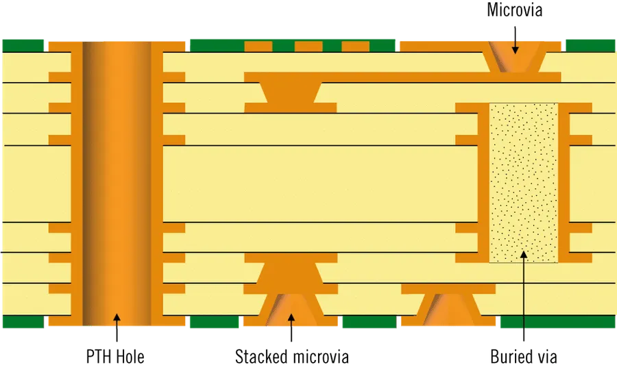
| Via Type and Count | Blind and buried vias are more expensive than through-hole vias due to additional processing steps. | Limit use of blind and buried vias; use through-hole vias where possible or strategically utilize microvias instead of buried vias. |
| Manufacturing Location | Manufacturing in regions with higher labor costs, like the USA or Europe, can be more expensive than in Asia. | Compare quotes from different regions, carefully considering lead times and communication efficiency with suppliers. |
| Design Complexity | Intricate designs with fine lines, small clearances, and unique features increase production costs and time. | Design for manufacturability (DFM) to minimize complexity. This involves simplifying the design where possible. |
| Order Volume | Low volume orders have higher per-unit costs due to setup and tooling charges. | Consolidate orders where possible to achieve quantity discounts. Consider panelization for small boards. |
Design for Manufacturability (DFM) is a key strategy for cost optimization. It involves designing the PCB with consideration for the manufacturing process. Implementing DFM practices can significantly reduce production costs by minimizing errors, reducing waste, and optimizing the manufacturing flow.
Frequently Asked Questions About Printed Wiring Board Manufacturing
This section addresses common queries regarding printed wiring board (PWB) manufacturing, providing clear and concise answers to enhance understanding of this critical aspect of electronics production. By exploring these frequently asked questions, we aim to clarify processes, technologies, and the overall PWB manufacturing landscape.
- Where are most printed circuit boards manufactured?
The majority of printed circuit boards (PCBs) are manufactured in Asia, particularly in China, Taiwan, and South Korea. These regions offer a combination of cost-effective labor, advanced manufacturing capabilities, and established supply chains, making them global hubs for PCB production. - Who designs printed circuit boards?
Printed circuit boards are primarily designed by electrical engineers and PCB design specialists. They use specialized software (CAD tools) to create the layout, ensuring that all electronic components can be interconnected effectively and the final product functions as intended. The design process is an iterative one, often requiring close collaboration with other engineering disciplines. - What are the latest innovations in PCB fabrication?
Recent innovations in PCB fabrication include the development of advanced materials with enhanced electrical and thermal properties, high-density interconnect (HDI) technology for miniaturization, additive manufacturing techniques (3D printing of PCBs), flexible and stretchable PCBs for unconventional applications, and eco-friendly materials and processes aimed at reducing the environmental footprint of electronics manufacturing. - Are printed wiring boards (PWBs) worth anything in their scrap form?
Yes, printed wiring boards (PWBs), in scrap form, possess inherent value due to the presence of precious metals such as gold, silver, copper, and palladium, which are used in their construction. These metals can be extracted and recycled. The economic viability of recycling PWBs depends on factors such as the concentration of these metals and the efficiency of recycling processes. - What is the typical lead time for manufacturing printed wiring boards?
Lead times for PWB manufacturing can vary significantly based on several factors, including the complexity of the board, order volume, the manufacturer's capacity, and any required special materials or processes. Standard lead times can range from a few days for simple prototypes to several weeks for complex, high-volume production runs. Expedited services are also available but typically incur additional cost. - How does the number of layers affect the cost of a printed circuit board?
The number of layers in a printed circuit board directly influences its manufacturing cost. As the layer count increases, the fabrication process becomes more complex, requiring additional steps for lamination, drilling, and plating. This complexity leads to increased material consumption, longer production times, and a higher cost per unit. Therefore, minimizing the number of layers while meeting the design requirements can be crucial for controlling expenses.
Future Trends in Printed Wiring Board Manufacturing
The printed wiring board (PWB) manufacturing sector is undergoing rapid transformation, driven by technological advancements and evolving market needs. Future trends point towards increased miniaturization, the rise of flexible substrates, and a strong focus on sustainable practices, alongside significant improvements in automation and assembly techniques.
- Miniaturization
The demand for smaller and more compact electronic devices is driving the need for higher density interconnect (HDI) PCBs. This includes finer lines and spaces, smaller vias, and more complex multilayer designs. Advances in lithography and etching techniques are crucial for achieving these levels of precision. - Flexible PCBs
Flexible printed circuit boards (FPCBs) are gaining traction due to their ability to conform to complex shapes and reduce the size and weight of electronic products. Materials science innovations are leading to improved performance and durability of these flexible substrates, while advanced manufacturing processes increase yield and reduce costs. - Sustainable Materials and Practices
Environmental concerns are pushing the industry towards more sustainable materials, including bio-based resins, and eco-friendly manufacturing processes. The goal is to reduce waste, energy consumption, and the use of hazardous materials during PCB production. These changes not only reduce environmental impact, but are also attractive to environmentally conscious consumers. - Advanced Assembly Automation
Automation and robotics are becoming indispensable in PCB assembly. Automated surface mount technology (SMT), pick-and-place machines, and advanced inspection systems enhance speed, accuracy, and consistency while reducing human error and production costs. These improvements are essential for producing more complex electronics while maintaining high quality. - Integration of AI and Machine Learning
Artificial intelligence (AI) and machine learning (ML) are increasingly being used to optimize manufacturing processes, detect defects, and improve overall yield. AI can assist with process control, predictive maintenance and automated quality checks. This adoption can lead to shorter lead times, reduced costs and better quality control in PCB manufacturing. - Embedded Components
Embedding components directly within the layers of the PCB rather than on the surface can lead to further miniaturization and increased functionality, which can result in higher device performance and improved protection and reliability. - 3D Printing in PCB Fabrication
Additive manufacturing techniques are being explored for PCB prototyping and even small-scale production, which could enable rapid turnaround and the production of customized, complex PCBs. Although not yet mainstream, 3D printing has the potential to revolutionize the manufacturing process by creating boards layer-by-layer.
Selecting the right printed wiring board manufacturers is critical for the success of any electronic product. By understanding the nuances of manufacturing capabilities, quality control, and cost considerations, you can make informed decisions that ensure your projects are backed by reliable and innovative solutions. Top printed wiring board manufacturers are constantly evolving, so staying informed is paramount for long-term success.