AnyPCBA PCB and PCBA case studies


Our client, a manufacturer of optical network equipment, needed a high-speed backplane for their next-generation optical transmission system. The backplane required exceptional signal integrity performance to support high-speed data transmission across a large board with thousands of differential signal pairs.
Key Technical Challenges:
High-Speed Signal Density: More than 320 differential pairs carrying 3.125G signals, plus over 640 additional differential pairs — totaling nearly 1,000 high-speed pairs
Large Form Factor: PCB size of 653 x 418mm, requiring precise manufacturing control to maintain flatness and signal integrity
Insertion Loss Management: Long trace lengths created significant insertion loss challenges that needed to be addressed through material selection and design optimization
Return Loss Control: Impedance mismatch risks throughout the long signal paths
Crosstalk and EMI: High-density routing with proximity between differential pairs created crosstalk and electromagnetic interference concerns
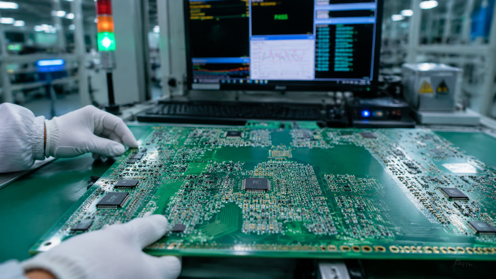
AnyPCBA provided comprehensive engineering support, from signal integrity simulation to PCB fabrication and assembly.
Our approach included:
3D Via and Trace Modeling: Used HFSS (High-Frequency Structure Simulator) to extract accurate via and trace models, enabling precise signal behavior prediction
Eye Diagram Simulation: Performed HSPICE simulations to verify signal quality at 3.125G data rates
S-Parameter Analysis: Analyzed insertion loss and return loss parameters to optimize impedance matching and minimize signal degradation
Material Selection: Recommended ultra-low-loss materials to meet insertion loss requirements over long trace lengths
Layer Stack Optimization: Optimized the layer stack and routing strategy to reduce the layer count from 32 to 28 layers while maintaining signal quality
Manufacturing Process Control: Implemented precise impedance control and back-drilling processes for the large 653 x 418mm board
| Parameter | Specification |
|---|---|
| Product Type | High-speed backplane for optical network |
| Signal Rate | 3.125G per channel |
| Differential Pairs | 320+ (3.125G) + 640+ (additional) |
| Board Size | 653 x 418 mm |
| Layer Count (Optimized) | 28 layers (reduced from 32) |
| Key Challenges | Insertion loss, return loss, crosstalk, EMI |
| Simulation Tools | HFSS, HSPICE |
Layer Reduction: Successfully reduced layer count from 32 to 28 layers — achieving approximately 12.5% cost savings while maintaining signal quality
Signal Integrity Verified: Eye diagram simulation and S-parameter analysis confirmed signal quality met performance requirements
Manufacturing Feasibility: Reduced layer count improved manufacturability and yield for the large-format board
Comprehensive Engineering Support: Provided full simulation, material selection, and fabrication services
One-Pass Success: Design optimization ensured first-pass success in fabrication and testing
This case demonstrates AnyPCBA's capability to handle demanding high-speed backplane and signal integrity challenges for optical network and telecommunications applications:
✅ High-speed signal integrity expertise (3.125G+, 320+ differential pairs)
✅ Advanced simulation capability (HFSS, HSPICE, S-parameter analysis)
✅ Large-format board manufacturing (653 x 418mm)
✅ Cost optimization through design (32→28 layer reduction)
✅ Ultra-low-loss material processing
Ready to discuss your high-speed backplane or optical network project? Contact us to learn how AnyPCBA can support your design and manufacturing needs.