Blog

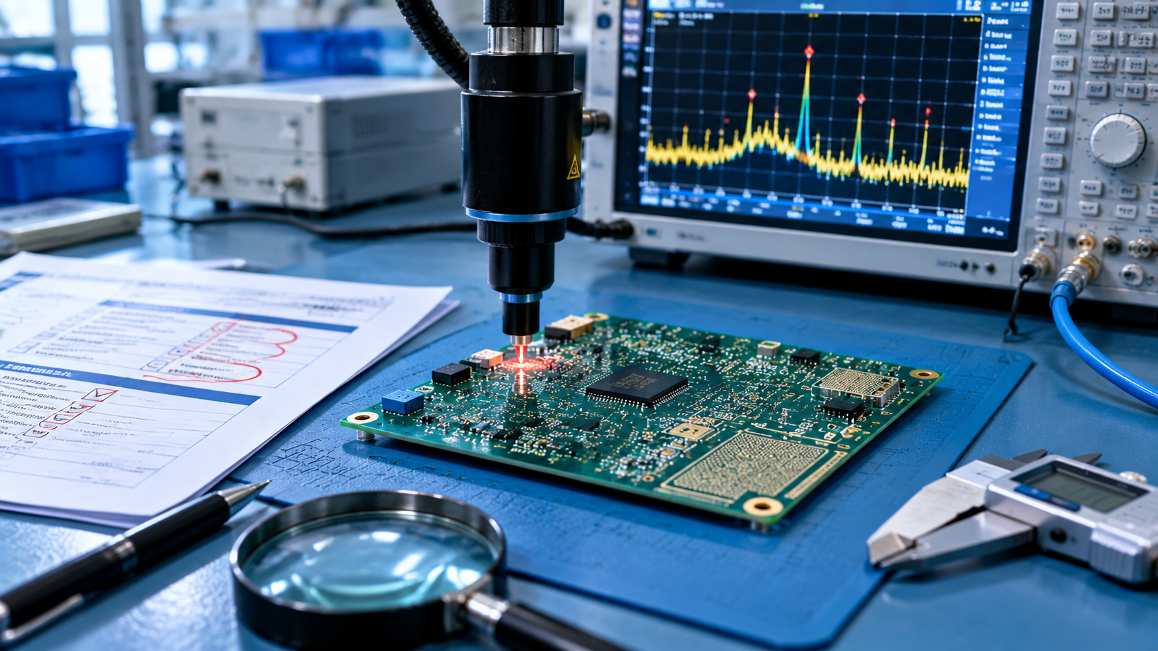
How to Reduce EMI and Optimize EMC in PCB Design – AnyPCBA

A practical guide to reducing EMI and optimizing EMC in PCB design. Covers EMI vs EMC, source classification, layout techniques, shielding, and external EMI suppression.
2026.09.14

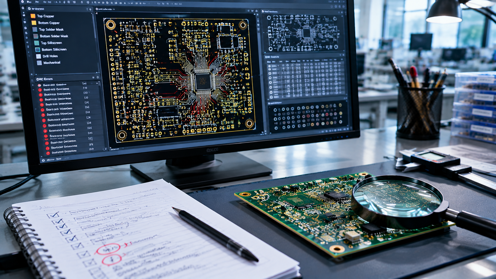
PCB Design Final Check Guide – Silkscreen, Drill, Mechanical & DRC Checklist – AnyPCBA

A practical checklist for final PCB design review before manufacturing. Covers silkscreen inspection, drill size and tolerance, mechanical checks, and DRC verification to avoid costly rework.
2026.09.14

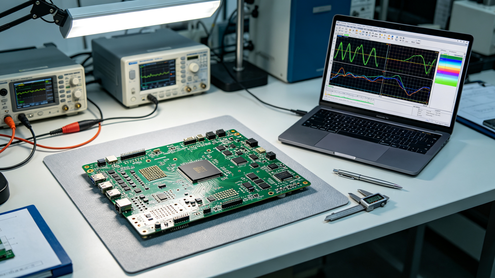
How to Improve High-Speed PCB Design Efficiency – SI/PI Simulation Guide – AnyPCBA

A practical guide to improving high-speed PCB design efficiency through SI/PI simulation. Covers design flow, pre-layout and post-layout analysis, and simulation tools for PCIe 6.0, USB4, and DDR5.
2026.09.11

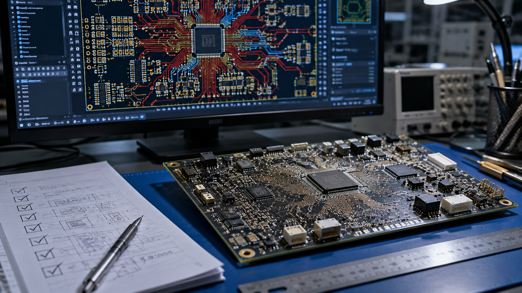
How Component Placement Reduces EMI – PCB Layout Guide – AnyPCBA

A practical guide to reducing EMI through proper PCB partitioning and component placement. Learn about return current paths, circuit zoning, and layout best practices for EMC compliance.
2026.09.11

Low EMI PCB Design Guide – Differential vs Common Mode Radiation – AnyPCBA

A practical guide to low EMI PCB design. Learn the difference between differential and common mode radiation, how to minimize loop area, and effective suppression techniques for EMC compliance.
2026.09.09

AI Server PCB Manufacturing Guide – Key Specs and Challenges – AnyPCBA

A technical guide to AI server PCB manufacturing. Covers extreme power density, 112G PAM4 signal integrity, back-drilling, thermal cycling reliability, and impedance control for high-performance AI hardware.
2026.09.09

Near-End vs Far-End Crosstalk – PCB Signal Integrity Guide – AnyPCBA

A comprehensive guide to near-end crosstalk (NEXT) and far-end crosstalk (FEXT) in PCB design. Learn about crosstalk mechanisms, measurement, and practical suppression techniques for high-speed digital designs.
2026.09.08

Common PCB Design Mistakes and Solutions – DFM Guide for Manufacturing – AnyPCBA

A practical guide to common PCB design mistakes that impact manufacturability. Learn how to avoid issues with test points, fiducial marks, panelization, component sourcing, and more.
2026.09.07

PCB Design Layout Guide – Complete PCB Layout Best Practices – AnyPCBA

A complete guide to PCB design layout best practices. Covers design rules, component placement, routing strategies, power/ground planes, thermal management, and DFM for manufacturable PCB designs.

2026.09.04

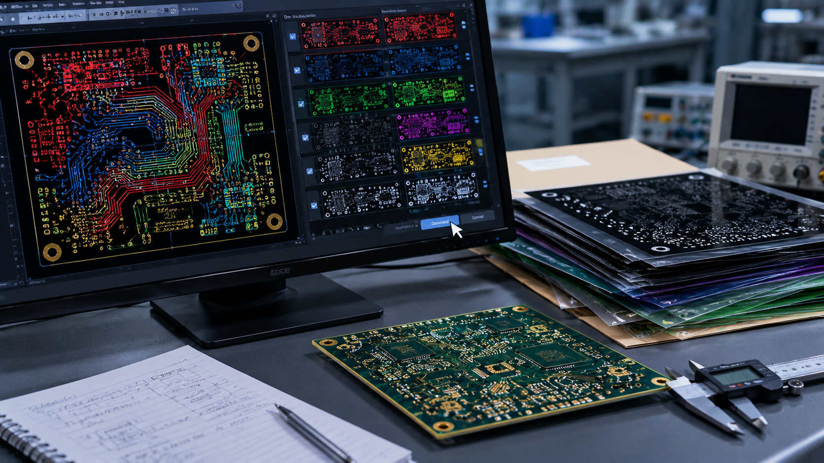
What Is a Gerber File in PCB Manufacturing? Complete Guide – AnyPCBA

A complete guide to Gerber files in PCB manufacturing. Learn about Gerber file structure, formats (RS-274X), generation process, validation, and common challenges for hardware engineers.
2026.09.03

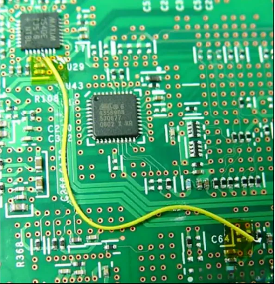
PCB Jumper Design Guide – Types, Applications, and Best Practices – AnyPCBA

A comprehensive guide to PCB jumper design. Learn about jumper types (wire, resistor, solder, PCB), common pitfalls, and design rules for reliable circuit connections.
2026.09.02

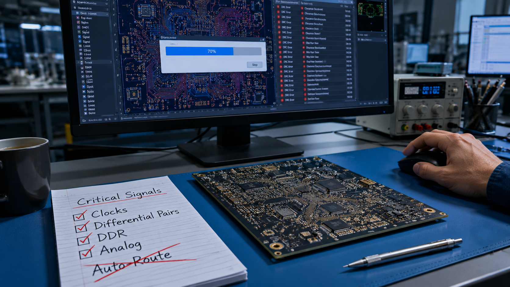
Why High-Speed PCBs Can't Be Fully Auto-Routed – A Practical Guide – AnyPCBA

A practical guide to high-speed PCB routing. Learn why auto-routing fails for high-speed designs, which signals require manual routing, and how to balance efficiency with signal integrity.
2026.09.01