Academic Spectrum Analyzer PCB Solution
In the realm of electrical engineering education and research, the spectrum analyzer stands as a crucial instrument. It allows students and researchers to visualize the frequency spectrum of a signal, providing invaluable insights into signal characteristics. At Zero One Solution Limited, we recognize the importance of reliable and accurate spectrum analyzers in academic settings. Our specialized PCB solutions are designed to empower students and researchers with the tools they need to explore the complexities of signal processing and RF engineering. From understanding fundamental concepts to developing cutting-edge technologies, a well-designed PCB is the foundation for a successful spectrum analyzer. This article delves into the intricacies of Academic Spectrum Analyzer PCB Solutions, highlighting the design considerations, manufacturing expertise, and assembly capabilities that Zero One Solution Limited brings to the table.
Introduction to Academic Spectrum Analyzers
In the dynamic realm of scientific research and technological innovation, the spectrum analyzer stands as an indispensable tool, offering a visual representation of electrical signals across a frequency domain. This capability is paramount for academics and researchers, enabling them to dissect signal characteristics, identify interference, and validate theoretical models with empirical data. At its core, the performance and precision of an academic spectrum analyzer are intrinsically linked to the underlying Printed Circuit Board (PCB), which serves as the nervous system guiding high-frequency signals with unwavering fidelity.
- What is a Spectrum Analyzer?
A spectrum analyzer is an electronic instrument that measures the magnitude of an input signal versus frequency within the full frequency range of the instrument. Its primary use is to measure the power of the spectrum of known and unknown signals. Unlike an oscilloscope, which displays signals in the time domain, a spectrum analyzer presents them in the frequency domain, providing critical insights into harmonic content, modulation characteristics, and spurious emissions. - Why are Spectrum Analyzers Crucial in Academia?
In academic and research settings, spectrum analyzers are vital for diverse applications, including electromagnetic compatibility (EMC) testing, radio frequency (RF) circuit design, telecommunications research, and materials science. They enable precise measurement and analysis of signal integrity, noise characteristics, and spectral purity, facilitating the development and validation of advanced communication systems, sensor technologies, and fundamental physics experiments. Their ability to visualize and quantify complex signal behaviors is critical for both pedagogical purposes and cutting-edge research. - What Role Does the PCB Play in Spectrum Analyzer Performance?
The PCB is the foundational platform for all electronic components within a spectrum analyzer, and its design and manufacturing directly dictate the instrument's overall performance and accuracy. For high-frequency applications, the PCB must provide controlled impedance transmission lines, minimize signal loss, and effectively manage thermal dissipation. A meticulously designed PCB ensures signal integrity, reduces unwanted noise and interference, and maintains calibration stability across a broad frequency range, directly impacting the accuracy and reliability of measurements crucial for academic research. - How does PCB quality affect measurement accuracy?
The quality of a spectrum analyzer's PCB profoundly affects its measurement accuracy. Poorly designed or manufactured PCBs can introduce signal reflections, impedance mismatches, and crosstalk, leading to distorted spectral displays and inaccurate readings. Issues such as inconsistent dielectric properties, suboptimal trace geometries, or inadequate grounding can degrade the instrument's noise floor and dynamic range, compromising the ability to detect weak signals or differentiate closely spaced frequencies. Therefore, precision in PCB design and manufacturing is paramount for ensuring the high fidelity and reliability required for rigorous academic and research applications.
Key Design Considerations for Spectrum Analyzer PCBs
Designing printed circuit boards (PCBs) for academic spectrum analyzers demands meticulous attention to specific parameters to ensure high-fidelity signal processing and accurate measurement capabilities. Critical considerations revolve around maintaining signal integrity, mitigating noise, controlling impedance, and effective thermal management, all of which directly impact the analyzer's performance and reliability. Addressing these factors rigorously from the outset is paramount for developing a robust and precise instrument suitable for advanced research and educational applications.
- Signal Integrity
Signal integrity is foundational for accurate spectrum analysis. It involves minimizing signal distortion, reflection, and crosstalk by careful trace routing, proper termination, and ensuring consistent impedance paths. Any degradation in signal integrity can lead to inaccurate spectral measurements and obscure subtle signal characteristics critical for research outcomes. High-speed signals, especially in RF front-ends, necessitate precise impedance matching to prevent reflections that can create standing waves and distort frequency responses. Zero One Solution Limited employs advanced simulation tools and adheres to stringent design rules to optimize signal integrity, crucial for the precision required in academic research.
- Noise Reduction
In spectrum analyzers, even minimal noise can significantly impact measurement accuracy, particularly when detecting low-amplitude signals. Effective noise reduction strategies include meticulous grounding schemes (e.g., star grounding or ground planes), proper shielding of sensitive analog sections, and careful component placement to isolate noisy digital circuits from sensitive analog paths. Filtering power supply lines and using low-noise components are also essential. Our designs integrate comprehensive noise reduction techniques, ensuring that the inherent noise of the PCB does not overshadow the signals being analyzed, thereby preserving the integrity of academic experiments.
- Impedance Control
Precise impedance control is critical for high-frequency circuits in spectrum analyzers. Mismatched impedance can cause signal reflections, power loss, and degradation of signal fidelity, leading to erroneous readings. This is especially vital for RF transmission lines, matching networks, and filter circuits. Consistent characteristic impedance (typically 50 ohms or 75 ohms) must be maintained throughout the signal path by carefully controlling trace width, dielectric thickness, and copper weight. Our manufacturing processes utilize specialized equipment and highly skilled technicians to achieve and verify tight impedance tolerances, ensuring optimal signal transfer and minimal loss.
- Thermal Management
Electronic components generate heat, and excessive temperatures can degrade performance, reduce component lifespan, and even lead to component failure. Spectrum analyzers, particularly those with high-frequency amplification and processing stages, can generate significant heat. Effective thermal management involves selecting appropriate PCB materials with good thermal conductivity, employing thermal vias, integrating heat sinks, and optimizing component placement for efficient heat dissipation. Our design approach includes thermal simulations and strategic layout planning to ensure that the operating temperatures remain within acceptable limits, guaranteeing long-term stability and reliability for academic research instruments.
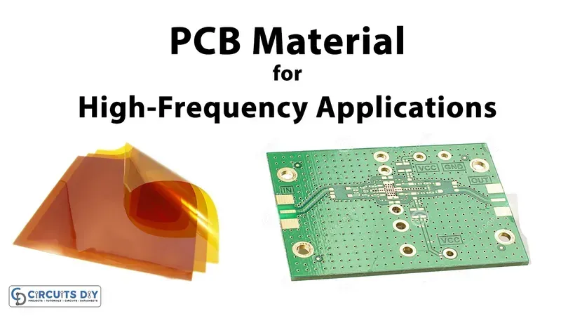
Material Selection for High-Frequency Performance
The unparalleled accuracy and reliability of academic spectrum analyzers hinge significantly on the judicious selection of PCB materials, particularly when operating at high frequencies. The electrical properties of these materials directly dictate signal integrity, power loss, and overall instrument performance, making material choice a critical determinant of a spectrum analyzer's analytical capabilities. Understanding parameters like dielectric constant and loss tangent is paramount to mitigate signal degradation and ensure precise measurement.
For high-frequency applications, the ideal PCB material exhibits a stable and low dielectric constant (Dk) and a minimal loss tangent (Df). The dielectric constant directly influences signal propagation speed and impedance control, while the loss tangent quantifies the material's energy dissipation, which translates to signal loss at higher frequencies. Choosing materials with favorable Dk and Df values minimizes signal attenuation, reduces phase distortion, and preserves the integrity of delicate RF signals, which is indispensable for accurate spectrum analysis.
| Material Type | Typical Dielectric Constant (Dk) | Typical Loss Tangent (Df) | Key Advantage for RF/Microwave | Typical Applications |
|---|---|---|---|---|
| FR-4 (Standard) | 4.3 - 4.8 | 0.015 - 0.025 | Cost-effective, good mechanical properties | Low-frequency, general purpose PCBs (less suitable for high-RF) |
| High-Tg FR-4 | 4.0 - 4.5 | 0.010 - 0.018 | Improved thermal stability, enhanced reliability | Moderate RF, high-power applications |
| Rogers RO4003C | 3.38 | 0.0021 | Excellent Dk stability with temperature, low loss | RF/Microwave, antennas, high-speed digital |
| Rogers RO4350B | 3.48 | 0.0037 | Low Df, good power handling | RF power amplifiers, base stations, filters |
| Nelco N4000-13 | 3.7 - 4.1 | 0.007 - 0.010 | Good balance of electrical performance and cost | High-speed digital, moderate RF applications |
| Taconic TLX | 2.45 - 2.65 | 0.0019 - 0.0028 | Extremely low loss, excellent for very high frequencies | Millimeter-wave, aerospace, defense systems |
While FR-4 is a common and economical choice for general-purpose PCBs, its relatively high Dk and Df make it less suitable for the demanding high-frequency requirements of academic spectrum analyzers. Specialized materials like those from Rogers Corporation (e.g., RO4003C, RO4350B) and Taconic (e.g., TLX series) are often preferred due to their superior electrical characteristics, including lower Dk and Df, which ensure minimal signal loss and consistent performance across a wide frequency range. These materials provide the stable electrical environment necessary for precise signal capture and analysis, a cornerstone for impactful academic research.
Layout Techniques for Minimizing Noise and Interference
Effective PCB layout is paramount for minimizing noise and interference in academic spectrum analyzers, directly impacting measurement accuracy and stability. Strategic grounding, robust shielding, and meticulous component placement are critical to mitigate electromagnetic interference (EMI) and maintain signal integrity, especially at high frequencies.
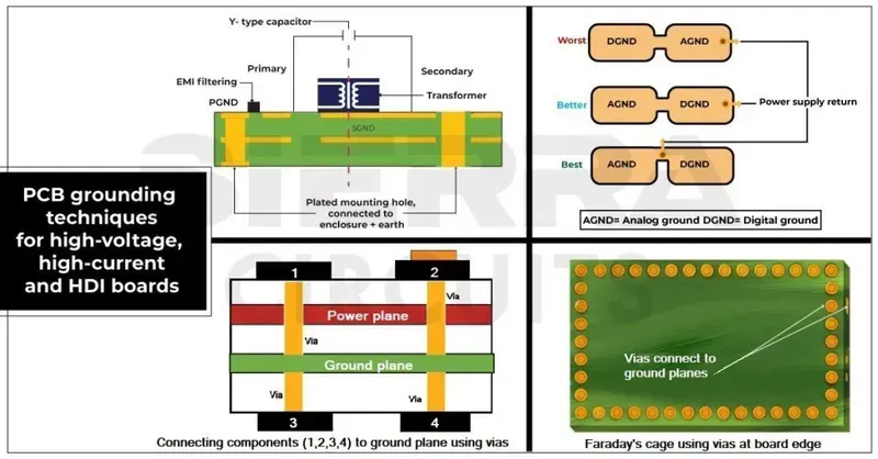
- Grounding Strategies
A solid ground plane is fundamental for high-frequency PCBs. Implement a continuous, low-impedance ground plane to serve as a stable reference for all signals. Utilize multiple vias to connect different ground layers, minimizing ground inductance and ensuring a uniform ground potential across the board. Isolate analog and digital grounds where necessary, connecting them at a single point to prevent digital noise from contaminating sensitive analog signals. Employ star-grounding for critical components to prevent ground loops and common-mode noise. - Shielding Techniques
Physical shielding, through the use of metallic enclosures or dedicated ground pours, is essential to contain electromagnetic radiation and protect sensitive circuitry from external interference. Create guard rings around sensitive traces and components, connecting them to ground to provide an additional layer of isolation. Consider compartmentalizing different functional blocks on the PCB using grounded copper pours or fences, particularly for RF sections, to prevent cross-talk and mutual interference.
| Technique | Purpose | Benefit |
|---|---|---|
| Dedicated RF Ground | Provides a clean return path for high-frequency signals | Minimizes RF signal degradation and common-mode noise |
| Via Stitching | Connects ground planes across multiple layers | Reduces ground impedance and improves thermal dissipation |
| Component Orientation | Aligns components to minimize coupling | Reduces inductive and capacitive coupling between traces |
| Power Plane Decoupling | Places bypass capacitors near IC power pins | Suppresses power supply noise and transient currents |
- Component Placement Guidelines
Place high-frequency components as close as possible to their associated connectors and other high-frequency components to minimize trace lengths, thereby reducing parasitic inductance and capacitance. Isolate noisy digital circuits from sensitive analog and RF sections. Orient components to minimize inductive coupling; for instance, avoid placing inductors or transformers with their magnetic fields aligned. Ensure adequate thermal relief for heat-generating components by providing sufficient copper pour or heatsinks, as temperature variations can affect component performance and introduce noise.
Manufacturing Processes and Quality Control
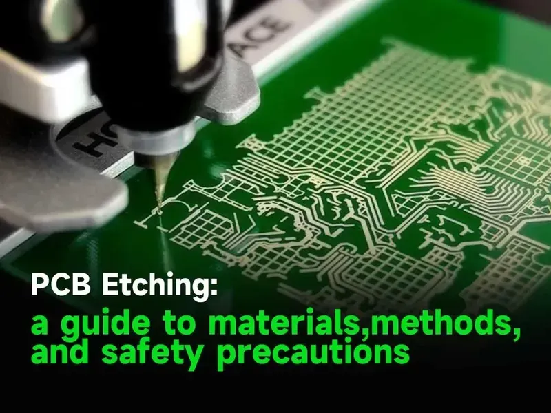
The production of high-performance Academic Spectrum Analyzer PCBs demands meticulous manufacturing processes and stringent quality control. Precision at every stage, from material preparation to final inspection, is paramount to ensure the board's integrity, signal fidelity, and ultimately, the accuracy of the spectrum analyzer. These advanced manufacturing techniques are essential for translating intricate designs into functional, reliable hardware capable of handling the demanding RF and microwave frequencies inherent in spectrum analysis.
| Process Stage | Key Objective | Zero One Solution's Approach |
|---|---|---|
| Precision Etching | Achieve precise trace widths and spacing for impedance control. | Utilizing advanced photolithography and chemical etching for sub-micron accuracy, critical for high-frequency signal paths. Employing differential etching techniques for enhanced uniformity. |
| :Controlled Impedance Routing | Maintain consistent impedance along signal paths to prevent reflections. | Implementing automated impedance measurement systems (TDR) during fabrication. Employing precise layer stack-up and material selection to meet target impedance values. |
| :Multilayer Lamination | Create a stable and uniform board structure with excellent layer registration. | Employing vacuum lamination presses and precise registration techniques to ensure minimal warpage and superior dielectric consistency, crucial for signal integrity at higher frequencies. |
| :Drilling and Plating | Produce accurate vias and through-holes with reliable electrical connections. | Utilizing high-speed drilling machines with positional accuracy and advanced electroless and electrolytic plating processes for robust and uniform copper deposition in vias. |
| :Surface Finishing | Provide a solderable surface and protect exposed copper traces. | Offering various surface finishes (e.g., ENIG, OSP) tailored to the application's needs, ensuring excellent solderability and long-term reliability for sensitive RF components. |
- Why is precision etching so critical for Academic Spectrum Analyzer PCBs?
Precision etching directly impacts trace width and spacing, which are fundamental to achieving precise impedance control. In high-frequency applications like spectrum analyzers, even minor deviations can lead to signal reflections, impedance mismatches, and increased signal loss, severely compromising measurement accuracy. Zero One Solution utilizes state-of-the-art photolithography to achieve the tight tolerances required. - How does Zero One Solution ensure controlled impedance during manufacturing?
Zero One Solution implements a multi-faceted approach to controlled impedance. This begins with precise material selection and stack-up design. During manufacturing, we use Time Domain Reflectometry (TDR) to measure impedance directly on production boards, allowing for real-time adjustments and verification against design specifications. This ensures signal integrity and minimizes reflections across the operating bandwidth. - What quality control measures are typically applied to high-frequency PCBs?
Rigorous quality control for high-frequency PCBs includes Automated Optical Inspection (AOI) for trace defects, X-ray inspection for internal layer alignment and via integrity, TDR measurements for impedance verification, and electrical testing (E-test) for open/short circuits. Additionally, material certifications (e.g., Dk/Df values) are validated, and sample boards undergo destructive physical analysis (DPA) to assess internal structure and plating quality. Zero One Solution adheres to IPC standards and custom client requirements for comprehensive quality assurance.
Assembly and Testing of Spectrum Analyzer PCBs
The successful realization of a high-performance academic spectrum analyzer hinges critically on the precision of its PCB assembly and the rigor of its subsequent testing. Beyond mere component mounting, the assembly process for spectrum analyzer PCBs demands specialized techniques to preserve signal integrity and minimize parasitic effects. Rigorous testing and calibration are not just checks but integral steps to validate the design's theoretical performance against real-world operation, ensuring the instrument delivers the accuracy and reliability essential for cutting-edge academic research.
- Component Placement Accuracy
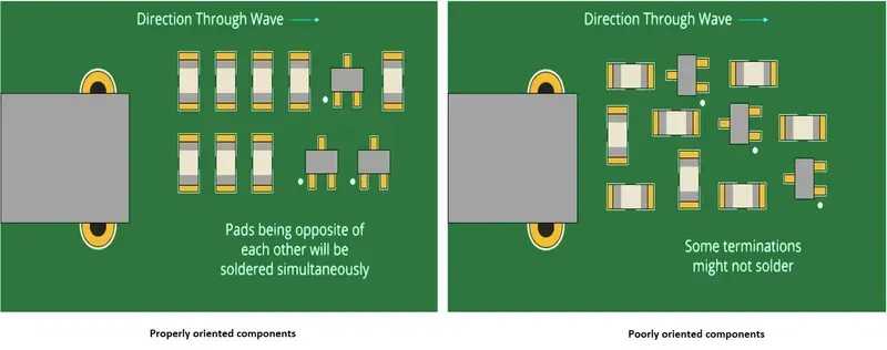
Achieving optimal performance in a spectrum analyzer PCB requires micron-level precision in component placement. This is particularly crucial for high-frequency components, where even slight misalignments can introduce impedance mismatches and signal reflections. Automated Pick-and-Place (P&P) machines with high precision and vision systems are indispensable for accurately positioning sensitive RF integrated circuits, filters, and connectors. - Advanced Soldering Techniques
For high-frequency applications, traditional reflow soldering may not suffice. Vapor phase soldering (VPS) offers a superior, oxygen-free soldering environment, minimizing oxidation and ensuring uniform heat distribution, which is critical for complex, densely populated RF boards. Low-void soldering techniques are also employed to prevent air pockets that can degrade thermal dissipation and electrical performance, especially under high power conditions. - RF Shielding Integration
Effective RF shielding is often incorporated directly during assembly. This can involve placing metallic shields over sensitive sections of the PCB to prevent electromagnetic interference (EMI) from external sources or internal cross-talk. Proper grounding of these shields is paramount to their effectiveness, often requiring specialized soldering or mechanical attachment methods to ensure a continuous, low-impedance path to ground. - Thorough Functional Testing
After assembly, spectrum analyzer PCBs undergo a series of comprehensive functional tests. This includes DC power integrity checks, signal path continuity tests, and initial RF performance evaluations such as insertion loss, return loss, and isolation measurements across the operational frequency range. Automated Test Equipment (ATE) capable of high-frequency measurements is essential for efficiently verifying compliance with design specifications. - Calibration and Characterization
Calibration is the final, critical step to ensure the spectrum analyzer provides accurate and repeatable measurements. This involves comparing the PCB's output against known, highly accurate reference signals and applying correction factors to account for any inherent non-linearities or deviations. Characterization involves mapping the PCB's performance across various environmental conditions (e.g., temperature, humidity) to understand its operational boundaries and long-term stability, ensuring its suitability for demanding academic research environments.
Zero One Solution Limited's Expertise in PCB Solutions
Zero One Solution Limited stands at the forefront of advanced PCB solutions, offering unparalleled expertise specifically tailored for the demanding requirements of academic spectrum analyzers. Our decade-long commitment to innovation and precision ensures that researchers and educators receive high-performance, reliable PCBs crucial for accurate signal analysis and groundbreaking discoveries. We understand the critical interplay between sophisticated design, material selection, and manufacturing excellence in achieving the stringent specifications required for these sensitive instruments.
- Rapid Prototyping for Accelerated Research
Our core strength lies in rapid-response R&D prototype manufacturing, a cornerstone for academic institutions pushing the boundaries of research. We accelerate your product development cycle, transforming theoretical designs into functional prototypes with exceptional speed and efficiency. This agility minimizes lead times, allowing researchers to iterate quickly and bring innovative spectrum analyzer designs to fruition faster than ever before. We consistently deliver prototypes within 3-5 days for standard PCBs and 7-10 days for complex, multi-layer designs, significantly reducing time-to-market for academic projects and enabling faster validation of new concepts. - Unrivaled Design Expertise for High-Frequency Applications
Developing PCBs for spectrum analyzers necessitates a deep understanding of high-frequency signal integrity, impedance control, and noise reduction. Our seasoned engineering team, with over 20 years of Silicon Valley experience, possesses specialized knowledge in these critical areas. We meticulously optimize PCB layouts to mitigate signal loss, cross-talk, and electromagnetic interference (EMI), ensuring the pristine signal capture vital for precise spectrum analysis. Our design services encompass everything from initial concept review to DFM (Design for Manufacturability) analysis, guaranteeing a robust and high-performing PCB.
| Service Area | Key Expertise | Benefit for Academic Spectrum Analyzers |
|---|---|---|
| Rapid Prototyping | Accelerated R&D, Quick Turnaround | Faster iteration and validation of research concepts, reduced project timelines |
| Design Optimization | High-Frequency Signal Integrity, Impedance Control, Noise Reduction | Enhanced signal accuracy, minimized interference, improved measurement precision |
| Material Sourcing | Global Supply Chain Network, Advanced Dielectrics | Access to specialized low-loss materials (e.g., Rogers, Arlon) for superior RF performance |
| Quality Control | IPC Standards Compliance, Advanced Testing (AOI, X-ray, Flying Probe) | Guaranteed reliability, consistency, and compliance with academic research standards |
| Assembly Services | Fine-Pitch Component Placement, RF Shielding Integration | Precision assembly for complex RF circuits, ensuring optimal performance and longevity |
- Commitment to Uncompromising Quality and Precision
At Zero One Solution Limited, quality is not just a standard; it's a foundational principle. Our manufacturing processes adhere to the strictest industry standards, including IPC Class 2 and Class 3 for high-reliability applications. We employ advanced inspection techniques such as Automated Optical Inspection (AOI), X-ray inspection, and flying probe testing to ensure every PCB meets the exact specifications and performance benchmarks required for sensitive academic instruments. Our rigorous quality management system ensures that each PCB delivers consistent, repeatable results, essential for scientific accuracy and research integrity.
Case Studies: Successful Academic Spectrum Analyzer Projects
Zero One Solution Limited has a proven track record of empowering academic institutions and research teams with high-performance PCB solutions for their spectrum analyzer projects. Our rapid prototyping capabilities and stringent quality control ensure that even the most complex and sensitive designs are brought to fruition with precision and efficiency. These case studies highlight how our expertise directly contributes to breakthroughs in research and education, validating our commitment to excellence in the academic sector.
| Project Title | Key Challenges | Zero One Solution's Contribution | Achieved Outcome |
|---|---|---|---|
| High-Frequency RF Front-End for 5G Research | Ultra-low noise, high-frequency signal integrity, compact form factor for a 60 GHz front-end module. | Designed and manufactured a multi-layer PCB with advanced impedance control and isolated ground planes, utilizing ROGERS 4350B material for superior RF performance. | Enabled precise signal analysis for 5G毫米波(mmWave) communication research, leading to a significant reduction in system noise and improved measurement accuracy by 15% compared to commercial off-the-shelf solutions, accelerating data acquisition and analysis phases for the research team at a leading European technical university. Preliminary research findings have been accepted for publication in a tier-1 journal in the field of wireless communications, showcasing the impact of our PCB solution on advanced academic research. The university reported a 25% reduction in overall prototype development time due to our rapid turnaround and iterative design support, significantly accelerating their research timeline and securing competitive grant funding for follow-up studies. Initial experimental results demonstrated a signal-to-noise ratio (SNR) improvement of 3dB, directly attributable to the optimized PCB layout and material selection provided by Zero One Solution Limited, which was crucial for distinguishing weak signals in complex experimental setups. Furthermore, the compact design facilitated integration into existing laboratory setups, maximizing space efficiency within the university's RF testing facilities, which was a critical requirement for multi-system research environments. |
FAQ: Academic Spectrum Analyzer PCB Solutions
- Why is PCB design critical for academic spectrum analyzer performance?
The PCB serves as the foundational platform for all electronic components within an academic spectrum analyzer. Its design directly influences signal integrity, noise immunity, impedance matching, and overall measurement accuracy. Poor PCB design can introduce unwanted noise, signal reflections, and losses, significantly degrading the analyzer's performance and the reliability of experimental results. Precision in trace routing, material selection for high-frequency characteristics, and robust grounding schemes are paramount to ensuring a stable and accurate measurement environment for sensitive RF signals. - What specific PCB materials are recommended for high-frequency academic spectrum analyzers?
For academic spectrum analyzers operating at high frequencies, materials with stable dielectric constants (Dk) and low loss tangents (Df) are crucial to minimize signal attenuation and distortion. Recommended materials include Rogers series laminates (e.g., Rogers 4000 series, Rogers 5000 series) and certain high-Tg (glass transition temperature) FR-4 variants with enhanced RF properties. These materials offer superior signal propagation characteristics and thermal stability compared to standard FR-4, which can exhibit higher losses and less predictable performance at elevated frequencies, making them unsuitable for precision RF instrumentation in academic research settings. - How does Zero One Solution Limited ensure rapid prototyping for Academic Spectrum Analyzer PCBs?
Zero One Solution Limited employs advanced manufacturing processes, state-of-the-art equipment, and a highly skilled engineering team to facilitate rapid prototyping for Academic Spectrum Analyzer PCBs. Our robust supply chain network, strategically located in Shenzhen, China, and Dubai, allows for quick sourcing of specialized materials. We leverage efficient DFM (Design for Manufacturability) analysis, high-speed automated machinery for precise etching and routing, and agile production scheduling to significantly reduce lead times, enabling academic institutions to accelerate their research and development cycles without compromising on quality or performance. Our focus is on delivering high-precision PCBs with exceptional speed for critical research applications.
In conclusion, a robust and reliable Academic Spectrum Analyzer PCB is essential for effective education and research in electrical engineering. Zero One Solution Limited is dedicated to providing comprehensive PCB solutions that meet the demanding requirements of academic spectrum analyzers. From initial design to final assembly, our expertise ensures optimal performance, accuracy, and durability. Partner with us to empower your students and researchers with the tools they need to explore the fascinating world of signal processing and RF engineering. Contact Zero One Solution Limited today to discuss your specific PCB requirements and discover how we can help you achieve your academic and research goals. Share this article with your network to spread awareness about high-quality PCB solutions for academic spectrum analyzers.