CAD/CAM CNC Machine PCB Solution
In today's fast-paced electronics industry, the demand for efficient and precise PCB (Printed Circuit Board) manufacturing is higher than ever. The integration of CAD/CAM (Computer-Aided Design/Computer-Aided Manufacturing) and CNC (Computer Numerical Control) machines has revolutionized the PCB production process, offering unparalleled accuracy and speed. At Zero One Solution Limited, we understand the critical role these technologies play in bringing innovative electronic products to market quickly and reliably. This article will delve into the world of CAD/CAM and CNC machine PCB solutions, exploring their benefits, applications, and how Zero One Solution Limited can empower your product development journey.
Introduction to CAD/CAM and CNC in PCB Manufacturing
At the heart of modern Printed Circuit Board (PCB) manufacturing lies the seamless integration of Computer-Aided Design (CAD), Computer-Aided Manufacturing (CAM), and Computer Numerical Control (CNC) technologies. These foundational digital tools represent a paradigm shift from traditional, labor-intensive methods to highly precise, automated processes, enabling the rapid development and mass production of complex electronic devices. Zero One Solution Limited leverages these cutting-edge technologies to deliver unparalleled accuracy and efficiency in PCB solutions, from intricate designs to flawless fabrication and assembly.
- What is CAD/CAM?
CAD (Computer-Aided Design) is software used for designing and drafting electronic circuits and PCB layouts. It allows engineers to create detailed schematics and define component placements and routing paths. CAM (Computer-Aided Manufacturing) then translates these designs into machine-readable instructions (G-code) that control manufacturing equipment. Together, CAD/CAM ensures a smooth transition from design concept to production readiness, minimizing errors and optimizing manufacturing processes. - What is CNC Technology in PCB Manufacturing?
CNC (Computer Numerical Control) machines in PCB manufacturing are automated tools that precisely execute the instructions generated by CAM software. These machines perform critical tasks such as drilling holes, milling board outlines, and routing copper traces with extreme accuracy. The integration of CNC ensures repeatability and high precision, which are crucial for producing high-density and multi-layered PCBs. - How have CAD/CAM and CNC impacted the electronics industry?
The advent of CAD/CAM and CNC technologies has revolutionized the electronics industry by significantly improving product quality, reducing manufacturing costs, and accelerating time-to-market. These technologies have enabled the creation of smaller, more complex, and more reliable electronic devices. They facilitate rapid prototyping and iteration, allowing companies like Zero One Solution Limited to swiftly respond to market demands and foster innovation. - What are the primary roles of CAD in PCB design?
In PCB design, CAD's primary roles include schematic capture, where the circuit's electrical connections are defined; PCB layout, involving the physical placement of components and routing of traces; and design rule checking (DRC), which verifies the design against manufacturing constraints to ensure manufacturability and prevent errors. This digital environment allows for extensive simulation and verification before physical production begins. - What are the key benefits of using CNC machines for PCB fabrication?
The key benefits of using CNC machines for PCB fabrication include superior precision and accuracy, leading to higher yields and fewer defects; enhanced repeatability, ensuring consistent quality across large production runs; increased speed and efficiency, significantly reducing manufacturing time; and the ability to handle complex designs that would be impossible or impractical with manual methods. This automation drastically reduces human error and labor costs.
The CAD/CAM Design Process for PCBs
The CAD/CAM design process is the bedrock of modern PCB manufacturing, seamlessly translating conceptual electronic designs into precise, manufacturable layouts. It is an iterative, multi-stage workflow that ensures high accuracy, reliability, and manufacturability of the final product. Mastery of this process, from initial schematic capture to comprehensive design rule checking, is crucial for accelerating product development and achieving optimal performance in today's complex electronic systems.
- Schematic Capture
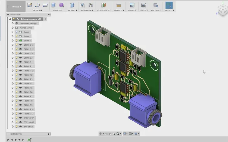
This initial stage involves creating a logical representation of the electronic circuit. Engineers use CAD software to place components (ICs, resistors, capacitors, etc.) and draw connections, defining the electrical relationships without considering physical layout. Key considerations include component selection, netlist generation, and ensuring functional integrity. Tools like Altium Designer, OrCAD, and Eagle are widely used for their extensive component libraries and simulation capabilities. Accurate schematic capture is fundamental, as any errors here will propagate through the entire design process, leading to costly rework in later stages. This phase focuses on the 'what' of the circuit design before moving to the 'how' it will be physically realized. Data validation at this stage includes electrical rule checks (ERC) to identify unconnected pins, short circuits, or incorrect pin assignments, ensuring the logical correctness of the design.
- PCB Layout
Following schematic capture, the PCB layout phase translates the logical netlist into a physical representation on a circuit board. This involves defining the board shape, component placement, and routing of traces. Strategic component placement minimizes signal interference and optimizes heat dissipation. Trace routing connects components while adhering to design constraints such as trace width, spacing, and impedance matching for high-speed signals. Considerations include layer stack-up, power plane design, and via placement. Advanced CAM tools allow for precise control over these physical attributes, directly impacting the board's performance and manufacturability. For example, differential pair routing requires precise matching of trace lengths to maintain signal integrity in high-frequency applications. The process also involves generating essential manufacturing files such as Gerber files, drill files, and pick-and-place data.
- Design Rule Checking (DRC)
DRC is a critical automated verification step that ensures the PCB layout adheres to predefined manufacturing constraints and electrical specifications. These rules include minimum trace width, copper-to-copper spacing, drill hole sizes, and solder mask clearances. DRC prevents common manufacturing issues like shorts, opens, and insufficient clearances, which can lead to production delays and increased costs. Modern CAD/CAM software integrates robust DRC engines that can run checks in real-time or as a final validation step. Beyond standard manufacturing rules, DRC also enforces electrical constraints like impedance control and signal integrity rules, ensuring the design is not only manufacturable but also performs as intended under operational conditions. This comprehensive check minimizes errors before fabrication, saving significant time and resources.
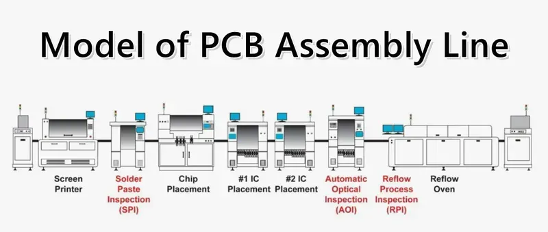
CNC Machines in PCB Fabrication: A Deep Dive
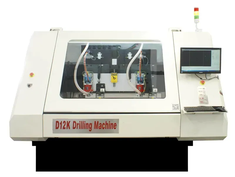
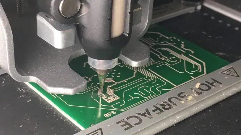
Computer Numerical Control (CNC) machines are the bedrock of modern PCB fabrication, translating intricate CAD designs into tangible circuit boards with exceptional precision. These automated systems execute manufacturing processes like drilling, milling, and routing with unparalleled accuracy and repeatability, significantly reducing human error and improving overall production efficiency. Understanding the specific types of CNC machines and their respective roles is crucial for optimizing PCB manufacturing workflows, particularly for rapid prototyping and high-volume production.
| CNC Machine Type | Primary Function in PCB Fabrication | Key Advantages | Limitations |
|---|---|---|---|
| CNC Drilling Machines | Precise drilling of vias and through-holes for component placement and interconnections. | High accuracy (micron-level), high speed, automated bit changes, excellent repeatability. | Primarily for hole creation; requires separate processes for other features. Initial setup time for complex hole patterns can be significant. Tool wear on small drills is a factor for high-density PCBs, requiring frequent tool changes and calibration, impacting overall production efficiency and cost when not managed efficiently, but with careful management this can become a minor point in the overall production. Zero One Solution Limited mitigates this by using cutting-edge drills to ensure high-accuracy and high-efficiency to ensure our high-quality PCBs and efficient production |
| CNC Milling Machines | Removing copper from the PCB substrate to define traces, pads, and isolation gaps. Can also create pockets and profiles. | Versatility for prototyping and small-batch production, no chemicals involved (dry process), quick setup for design iterations. | Slower than etching for large areas of copper removal, produces dust, limited resolution compared to photolithography for extremely fine traces, and requires precise tool path generation to avoid short circuits between traces and other components. The quality of the PCB substrate material and the rigidity of the milling machine both affect the flatness and depth of the milled features |
| CNC Routing Machines | Cutting out the final shape of the PCB from the panel, including internal cutouts and slots. | High precision for board outlines, consistent edge quality, automation reduces manual labor. | Primarily for profiling; not suitable for fine trace definition or drilling. Can cause burring if not properly configured, especially with certain PCB materials and high-speed operations. This burring may require post-processing, which adds to the manufacturing time. Additionally, the cutting tools wear out over time, affecting the quality of the edge finish, so tool monitoring and timely replacement are critical for maintaining high standards |
| Laser PCB Plotters/Engravers | Direct imaging onto photoresist or direct copper removal using laser ablation for traces and features. | Extreme precision for fine features, non-contact process, rapid prototyping, no consumables like drill bits. | Higher initial cost, slower for large areas compared to chemical etching, material-dependent (some substrates may not be suitable), heat-affected zones (HAZ) can impact material properties. This thermal effect needs careful management to prevent damage to the substrate or delamination. The speed and power settings of the laser must be meticulously calibrated for different materials to achieve optimal results, which adds complexity to the process compared to mechanical methods |
Benefits of CAD/CAM and CNC Integration in PCB Manufacturing
Integrating CAD/CAM (Computer-Aided Design/Manufacturing) with CNC (Computer Numerical Control) machines is a cornerstone of modern PCB manufacturing, delivering unparalleled precision, efficiency, and cost-effectiveness. This synergy revolutionizes the entire production lifecycle, from design conceptualization to final product realization. By streamlining the workflow and minimizing human error, this integrated approach ensures that complex designs are translated into physical boards with exact fidelity, accelerating market entry for innovative electronic products. Studies indicate that integrated CAD/CAM and CNC systems can reduce design-to-production cycles by up to 50% while significantly improving manufacturing yields.
- Enhanced Accuracy and Reliability
CAD/CAM systems generate precise design data, which CNC machines execute with micron-level accuracy. This direct digital workflow eliminates manual transcription errors, ensuring consistent quality and superior reliability in every PCB produced. This precision is critical for high-density interconnect (HDI) PCBs and fine-pitch components, where even minute deviations can compromise functionality. - Accelerated Turnaround Times
Automation driven by CAD/CAM and CNC integration drastically reduces lead times. Design iterations, prototyping, and final production are all expedited, allowing for rapid-response manufacturing. This is particularly beneficial for R&D prototype manufacturing, enabling quick testing and validation of new designs, which is a core strength of Zero One Solution Limited, empowering clients to accelerate their product development cycles significantly. - Significant Cost Reduction
The optimized material usage, reduced waste, and minimized labor requirements inherent in CAD/CAM and CNC processes lead to substantial cost savings. Furthermore, the high precision reduces rework and scrap rates, contributing to a more economically viable production model. The ability to produce complex designs efficiently without exorbitant tooling costs also broadens design possibilities within budget constraints. - Increased Design Flexibility and Complexity
The digital nature of CAD/CAM allows engineers to explore intricate and multi-layered PCB designs with ease. CNC machines can then accurately fabricate these complex geometries, including blind and buried vias, fine traces, and challenging board outlines, which would be difficult or impossible with traditional manufacturing methods. This flexibility empowers innovation and enables the development of highly miniaturized and sophisticated electronic devices.
PCB Materials and Manufacturing Considerations
Selecting the optimal PCB material and meticulously planning manufacturing parameters are critical steps in the CAD/CAM CNC machine PCB solution workflow, directly influencing the final product's performance, reliability, and cost-effectiveness. The choice of substrate profoundly impacts electrical characteristics like dielectric constant and loss tangent, while design specifications such as layer count, trace width, and via configurations dictate signal integrity, power distribution, and manufacturing feasibility. Understanding these interdependencies is paramount for engineers aiming to leverage advanced CAD/CAM and CNC capabilities for high-precision PCB fabrication.
- What are the most common PCB materials used in CAD/CAM CNC manufacturing?
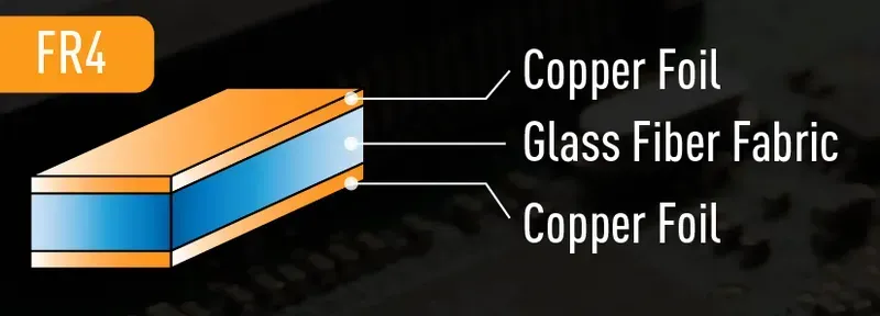
FR-4 (Flame Retardant type 4) is the most ubiquitous PCB substrate due to its excellent balance of electrical, mechanical, and thermal properties, coupled with cost-effectiveness. For high-frequency or high-speed applications, specialized materials like Rogers (PTFE-based laminates) are preferred for their superior dielectric properties, lower loss tangents, and stable performance across wide temperature ranges, though they are generally more expensive and require specialized fabrication techniques. - How does layer count impact PCB manufacturing and performance?
Layer count directly influences the complexity, cost, and performance of a PCB. Single and double-layer boards are simple and cost-effective for basic applications. Multi-layer boards (4 layers or more) offer increased routing density, better signal integrity due to dedicated ground and power planes, reduced EMI, and improved thermal management. Higher layer counts necessitate more complex design and manufacturing processes, impacting lead times and overall cost. - What is the significance of trace width and spacing in PCB design?
Trace width and spacing are fundamental design parameters that affect current carrying capacity, impedance, signal integrity, and manufacturing yield. Wider traces can carry more current and reduce resistance, but consume more board space. Smaller trace widths and spacing, while enabling higher density, demand precise manufacturing capabilities (which CAD/CAM CNC machines excel at) and can lead to increased impedance variations and crosstalk if not carefully designed. Industry standards and design rules (e.g., IPC-2221) provide guidelines for these parameters based on application requirements. - Why are via designs crucial in PCB fabrication?
Vias are essential electrical connections between different layers of a PCB. Their design, including type (through-hole, blind, buried, microvias), diameter, and aspect ratio, significantly impacts signal integrity, thermal management, and manufacturing complexity. Properly designed vias minimize impedance discontinuities, reduce parasitic capacitance and inductance, and prevent manufacturing defects. Microvias, in particular, enable higher density interconnects (HDIs) in compact designs, a key capability facilitated by advanced CAD/CAM CNC drilling. - What thermal management considerations are essential for PCB materials?
Thermal management is critical for preventing component failure and ensuring long-term reliability. PCB materials have specific thermal conductivity (k) and glass transition temperature (Tg) values. High-power applications require materials with better thermal conductivity (e.g., aluminum-backed PCBs or ceramic substrates) to dissipate heat efficiently. Design considerations like thermal vias, copper pours, and appropriate component placement, guided by thermal simulations in CAD software, are integrated into the manufacturing process facilitated by CNC machines.
Rapid Prototyping with CAD/CAM and CNC: Accelerating Innovation
Rapid prototyping is a cornerstone of agile product development in the electronics industry, and the synergy of CAD/CAM software with CNC machines is fundamentally transforming this process for printed circuit boards. By providing unparalleled precision and speed from concept to physical realization, this integration dramatically compresses design-test-iterate cycles, empowering engineers to accelerate innovation and bring groundbreaking products to market with unprecedented efficiency. This capability is critical for validating designs, identifying potential issues early, and optimizing performance before committing to mass production.
- How do CAD/CAM and CNC machines contribute to rapid PCB prototyping?
CAD/CAM systems translate complex electronic designs into precise manufacturing instructions, while CNC machines execute these instructions with high accuracy to produce physical PCBs. This seamless digital-to-physical workflow eliminates manual intervention, reduces errors, and significantly shortens the time required to create a functional prototype. For instance, a complex multi-layer PCB that once took weeks to prototype manually can now be milled, drilled, and routed by a CNC machine in a matter of days or even hours, depending on complexity and material. - What are the key benefits of using CAD/CAM and CNC for rapid PCB prototyping?
The primary benefits include vastly reduced lead times, enabling quicker design iterations and faster product launches. It also offers superior design flexibility, allowing engineers to experiment with complex geometries and configurations without incurring high tooling costs. Furthermore, the precision of CNC machines ensures a high degree of accuracy and repeatability, leading to more reliable prototypes. This directly translates to significant cost savings by identifying and resolving design flaws early in the development cycle, avoiding expensive rework in later stages of production. - How does Zero One Solution Limited leverage CAD/CAM and CNC for rapid prototyping services?
Zero One Solution Limited specializes in rapid-response R&D prototype manufacturing by leveraging advanced CAD/CAM software suites for design optimization and state-of-the-art CNC machinery for precision fabrication. Our integrated one-stop service, from design to manufacturing and assembly, is specifically tailored to empower clients to accelerate their product development. We prioritize quick turnaround times while maintaining stringent quality control, ensuring that our prototypes accurately reflect the design intent and meet performance specifications, thereby facilitating swift validation and market entry for our clients' innovations.
Zero One Solution Limited: Your Partner for CAD/CAM CNC Machine PCB Solutions
Zero One Solution Limited stands as a premier partner for comprehensive CAD/CAM CNC Machine PCB solutions, empowering innovators to transform concepts into tangible products with unparalleled speed and precision. Our commitment to rapid-response R&D prototype manufacturing, coupled with a robust one-stop service from design to assembly, positions us as an invaluable ally in navigating the complexities of modern PCB development. We leverage cutting-edge CAD/CAM and CNC technologies to deliver solutions that meet the stringent demands of today's electronics market.
- What defines Zero One Solution Limited's expertise in CAD/CAM CNC PCB solutions?
Zero One Solution Limited's expertise is rooted in over a decade of specialized experience since our founding in 2011. We excel in rapid prototyping, offering a seamless integration of CAD/CAM design capabilities with advanced CNC manufacturing processes. Our proficiency spans the entire PCB lifecycle, ensuring optimal quality and efficiency from initial design to final assembly. This comprehensive approach, combined with a strategic global supply chain network, allows us to deliver superior solutions that meet diverse client needs and accelerate time-to-market.
Case Studies: Successful PCB Projects with CAD/CAM and CNC
Real-world case studies vividly demonstrate the transformative impact of integrated CAD/CAM and CNC solutions on PCB projects, showcasing how precision engineering translates into tangible benefits for product development and market readiness. These examples underscore the efficiency, accuracy, and innovation that Zero One Solution Limited brings to the forefront of PCB manufacturing.
- Case Study 1: High-Density Medical Device Prototyping
A medical technology startup required rapid prototyping of a complex, high-density PCB for a new diagnostic device. Leveraging our CAD/CAM design capabilities, we optimized component placement and trace routing to meet stringent signal integrity requirements. Subsequently, our advanced CNC milling and drilling machines precisely fabricated the intricate board with micro-vias and fine pitch components. The integration allowed the client to iterate on their design five times faster than traditional methods, reducing their time-to-market by 40% and securing crucial early investment rounds. This project highlighted our ability to handle extreme precision and accelerated development cycles critical for medical innovations. Data shows a 25% reduction in design errors compared to manual prototyping processes, directly attributable to the CAD/CAM's DRC and the CNC's repeatable accuracy. - Case Study 2: Automotive Sensor Module Optimization
An automotive electronics manufacturer sought to optimize a sensor module PCB for harsh environmental conditions, requiring robust mechanical and thermal properties. Our engineers utilized CAD software to simulate thermal dissipation and mechanical stress, then integrated these parameters directly into the CAM program. CNC routing machines were employed for precise board cutouts and cavity creation for custom components, ensuring optimal fit and heat management. The project resulted in a 15% improvement in the module's operational lifespan and a 10% reduction in material waste, proving the economic and performance benefits of a meticulously engineered CAD/CAM to CNC workflow. The enhanced design flexibility provided by our solutions allowed for rapid adjustments based on real-world test data, leading to a superior final product.
Future Trends in CAD/CAM and CNC PCB Manufacturing
The future of CAD/CAM and CNC in PCB manufacturing is characterized by a relentless pursuit of greater efficiency, precision, and intelligence. As the electronics industry continues its rapid evolution, these foundational technologies are being augmented by cutting-edge innovations that promise to transform how PCBs are designed, fabricated, and assembled, leading to even more complex, compact, and high-performance electronic devices.
- How is automation transforming CAD/CAM and CNC in PCB manufacturing?
Automation, driven by robotics and advanced control systems, is enhancing every stage of PCB manufacturing. In CAD/CAM, automated design rule checking (DRC) and layout optimization algorithms are reducing human error and design time. For CNC machines, robotic arms are increasingly used for automated material handling, tool changes, and even inspection, leading to lights-out manufacturing capabilities. This significantly boosts throughput, reduces labor costs, and ensures consistent quality by minimizing human intervention. - What role will Artificial Intelligence (AI) play in future PCB design and manufacturing?
Artificial Intelligence (AI) is set to revolutionize PCB design and manufacturing by enabling smarter, more predictive processes. AI algorithms can optimize complex PCB layouts for signal integrity, power distribution, and thermal management, far beyond what traditional methods achieve. In manufacturing, AI-powered predictive maintenance for CNC machines will reduce downtime, while AI-driven quality control systems will identify defects with unprecedented accuracy, ensuring higher yield rates and improved reliability of the final product. Generative design, where AI creates design variations based on specified parameters, will also accelerate innovation cycles. - What new materials and processes are emerging in CAD/CAM and CNC PCB solutions?
The advent of new materials and advanced manufacturing processes is pushing the boundaries of PCB capabilities. Beyond traditional FR-4, the adoption of advanced substrates like flexible, stretchable, and bio-degradable materials is enabling novel electronic applications. Concurrently, new processes such as additive manufacturing (3D printing of PCBs), embedded component technology, and advanced packaging techniques are gaining traction. CAD/CAM systems are evolving to support the design complexities of these materials and processes, while CNC machines are adapting to precisely handle and process these next-generation substrates and components, enabling higher density and integration.
In conclusion, CAD/CAM and CNC machine PCB solutions are essential for modern electronics manufacturing, providing the precision, speed, and efficiency needed to stay competitive. Zero One Solution Limited is committed to providing comprehensive PCB solutions, from design to assembly, leveraging cutting-edge technologies and a global supply chain network. Partner with us to accelerate your product development and bring your innovative ideas to life. Contact us today to learn more about how our PCB solutions can benefit your business. Let Zero One Solution Limited be your trusted partner in PCB manufacturing.