Choosing the Right PCB CAD Software: A Comprehensive Guide
In our increasingly interconnected world, printed circuit boards (PCBs) are the unsung heroes powering nearly all of our electronic devices. From the smartphones in our pockets to the sophisticated medical equipment in hospitals, these intricate boards rely on precision design enabled by PCB CAD software. Choosing the right PCB CAD tool is critical for hobbyists and professionals alike, impacting efficiency, design accuracy and overall product success. This article delves into the varied landscape of PCB CAD options, providing actionable insights to help you navigate this critical design space and master the creation process.
Understanding PCB CAD: What It Is and Why It Matters
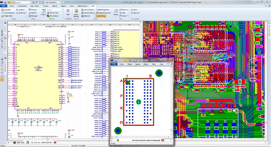
PCB CAD, or Printed Circuit Board Computer-Aided Design, is a specialized software domain focused on the design and layout of electronic circuits. Unlike general CAD software like AutoCAD, which deals with mechanical or architectural designs, PCB CAD is specifically tailored for creating the intricate patterns of conductive traces, vias, and component placements required for functional electronic circuit boards.
At its core, PCB CAD software empowers engineers and designers to translate abstract circuit schematics into physical layouts that can be manufactured. It provides a suite of tools that streamline the design process, significantly reducing manual effort and minimizing errors. This ensures the reliable, efficient, and accurate creation of complex electronic systems.
The advantages of using PCB CAD software are manifold. It allows for the rapid prototyping and modification of designs, which are vital in today's fast-paced electronics industry. These tools facilitate accurate component placement, ensure proper signal integrity through precise trace routing, and enable the generation of manufacturing files directly, optimizing the transition from design to production.
Key Features to Look for in PCB CAD Software
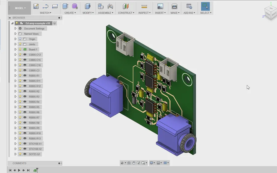
Selecting the appropriate PCB CAD software is crucial for efficient and accurate circuit board design. The ideal software should offer a robust set of features that streamline the design process, from schematic capture to final layout. Core functionalities include precise component placement, effective routing, comprehensive component libraries, simulation capabilities, and clear 3D visualization, which enhances the user's ability to assess the mechanical and spatial aspects of their designs. Ultimately, a balance of functionality and an accessible user interface is key to optimizing productivity and minimizing errors.
| Feature | Description | Importance |
|---|---|---|
| Schematic Capture | The ability to create and edit electronic circuit diagrams. It involves placing components, connecting them with wires, and assigning values and parameters. | Essential for defining the electrical connections and relationships between components. It provides the foundation for the PCB layout. |
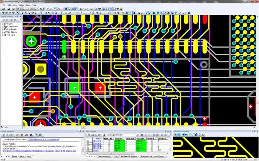
| PCB Layout | Tools for designing the physical arrangement of components on the circuit board, including trace routing, pad placement, and copper pours. | Critical for translating the schematic into a manufacturable physical design. Effective layout ensures optimal electrical performance and signal integrity. |
| Routing Capabilities | Functionality for creating connections between components using copper traces. Includes features for automatic routing, manual routing, and via placement. | Efficient routing is key for signal integrity and minimizing electromagnetic interference. Good routing capabilities can significantly reduce design time and costs. |
| Component Libraries | A collection of pre-defined components with their physical and electrical characteristics. The library should be comprehensive and regularly updated. | Extensive and accurate libraries are essential for error-free designs and can save significant design time. |
| Simulation Tools | Tools that can simulate the behavior of the designed circuit, including signal analysis, thermal analysis, and electromagnetic compatibility. | Simulation capabilities help designers identify potential issues and optimize designs before manufacturing, thereby reducing the risk of costly errors and delays. |
| 3D Visualization | The ability to display the design in three dimensions. This helps designers verify mechanical fit and assess the spatial relationship between components. | 3D visualization is valuable for mechanical design checks and improves the understanding of the final assembled PCB. |
| User Interface and Ease of Learning | The overall user experience and the ease with which a new user can start to use the tool. | An intuitive user interface and well-structured workflow are important for minimizing the learning curve and ensuring an efficient design process. |
Top PCB CAD Software Options: A Comparative Analysis
Selecting the appropriate PCB CAD software is crucial for efficient and effective circuit board design. This section provides a comparative analysis of leading software options, highlighting their strengths, weaknesses, pricing structures, and suitability for various user profiles. Our aim is to furnish a clear understanding of the landscape, enabling informed decisions tailored to specific project needs and budgetary constraints. We will delve into the functionalities of popular tools, ranging from industry-standard solutions to accessible open-source alternatives.
| Software | Strengths | Weaknesses | Pricing Model | Target User Group |
|---|---|---|---|---|
| Altium Designer | Industry-standard, comprehensive features, powerful routing capabilities, extensive component libraries. | High cost, steep learning curve for beginners. | Subscription-based | Professionals, large-scale projects, complex designs. |
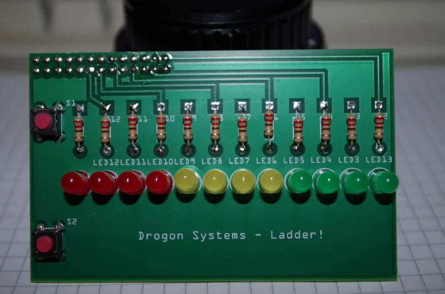
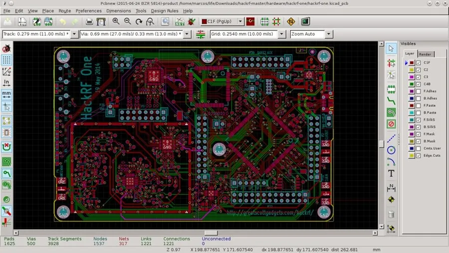
| KiCad | Open-source, free, active community, robust feature set, cross-platform compatibility. | Less polished interface compared to commercial options, may require more user configuration. | Free | Hobbyists, students, small to medium-sized projects, open-source enthusiasts. |
| Autodesk EAGLE | Integrated with Fusion 360, good balance of features and price, user-friendly interface, available in free version. | Limited features in free version, can be less powerful than Altium for advanced designs. | Subscription-based, Free version available | Hobbyists, small to medium-sized businesses, maker community, educational users |
| EasyEDA | Free online platform, intuitive interface, suitable for beginners, easy collaboration, integrates with LCSC for component sourcing. | Limited features compared to desktop software, dependent on internet connectivity, less powerful for complex multilayer PCBs. | Free with optional paid features | Hobbyists, beginners, small projects, rapid prototyping, educators. |
| CircuitMaker | Free, community-driven, cloud-based, good balance of features, user friendly interface | Less features than Altium, potential for instability compared to desktop software | Free | Hobbyist, small scale professional projects. |
| DipTrace | User-friendly interface, moderate pricing, 3D visualization, good for mid-level complexity designs. | Fewer advanced features compared to Altium, less community support than KiCad. | Perpetual licenses available | Small to medium-sized projects, companies looking for moderate pricing and easy to use software |
| ExpressPCB | Extremely easy to learn, very simple interface, seamless integration with their fabrication services | Limited design capabilities, no Gerber output, tied to their fabrication services | Free to use with manufacturing | Very simple projects, single layer PCBs, users who require a very quick turnaround |
Free vs. Paid PCB CAD Software: Which is Right for You?
Selecting the appropriate PCB CAD software often involves a crucial decision: opting for a free or a paid solution. This choice is not solely determined by cost but also by the complexity of your projects, required functionalities, and the level of support needed. Understanding these differences is essential to ensure that the selected software aligns with your design requirements and budget.
| Feature | Free PCB CAD Software | Paid PCB CAD Software |
|---|---|---|
| Cost | No or minimal upfront cost. | Significant upfront or subscription costs. |
| Functionality | Basic features suitable for simple to moderately complex designs. May have limitations on design size or layers. | Advanced features for complex designs, including advanced routing, simulation, and analysis tools. Generally no limitations on design size or layers. |
| Component Libraries | May have limited, community-driven or less comprehensive component libraries. | Usually offer vast, professionally maintained component libraries. |
| Support | Community-based support forums and documentation. Often limited formal support. | Dedicated support channels, documentation, and tutorials. Faster response times. |
| Updates and Maintenance | May have less frequent or less rigorously tested updates. | Regular updates, bug fixes, and feature enhancements are provided. |
| Target Users | Hobbyists, students, and small-scale projects. | Professional engineers and enterprises handling complex projects. |
| Customization | Limited customization options. | Offers more extensive customization and scripting options. |
| Integration | May have limitations in integration with other design tools. | Often seamless integration with other design and manufacturing tools. |
The decision between free and paid PCB CAD software hinges on a balance between cost, functionality, and required support. Free options are excellent for learning, hobbyist projects, and simple designs, while paid options are geared towards complex, high-reliability designs that professional engineers often require. Carefully assess your needs to make the most appropriate choice.
PCB CAD Software for Specific Needs: Hobbyists, Students, and Professionals
The selection of PCB CAD software is highly dependent on the user's specific needs, experience level, and project complexity. Different software packages cater to hobbyists, students, and professionals, each with distinct requirements in terms of features, learning curve, and cost. This section provides tailored recommendations to guide each user group towards the most suitable options.
For **hobbyists**, the primary focus is often on ease of use and cost-effectiveness. Many hobbyist projects are less complex, focusing on learning and experimentation rather than intricate design. Therefore, features such as intuitive interfaces, readily available tutorials, and free or low-cost options are crucial.
- Recommended Software for Hobbyists
KiCad stands out as a robust, open-source option that offers a wide range of features without any cost. Its large community support and availability of online resources make it excellent for beginners. EasyEDA, a cloud-based tool, provides a user-friendly interface and strong community support, ideal for simpler projects, and is free for most users.
For **students**, educational institutions often require software that supports learning the fundamental principles of PCB design, but the budget can be limited. The software should offer features for schematic design, layout, and basic simulation to facilitate understanding the overall process.
- Recommended Software for Students
KiCad continues to be suitable given its open-source nature and complete feature set. Autodesk EAGLE, while requiring a subscription, provides student licenses, making it accessible for educational purposes, and industry relevance as many professionals use EAGLE . Additionally, some universities may utilize specific software as part of their curriculum, aligning training with practical industry tools.
For **professionals**, the emphasis shifts to software that can handle complex, high-density, and high-speed designs. These tools must offer advanced routing capabilities, strong simulation and analysis features, seamless integration with other design tools, and robust support. Time and efficiency in producing top-notch PCBs are key, and thus, cost becomes a secondary concern.
- Recommended Software for Professionals
Altium Designer is an industry-leading choice due to its comprehensive feature set, including sophisticated routing, simulation, and data management capabilities. While the most expensive option, it is a professional standard and can handle advanced design projects. Mentor Graphics' Xpedition is another high-end solution, often utilized by large companies for complex multilayer designs, and it integrates easily with other design tools. Cadence Allegro is a professional-level option with advanced analysis and routing features, and is also often used in large companies with a focus on high speed/density designs.
| User Group | Primary Needs | Recommended Software Options |
|---|---|---|
| Hobbyists | Ease of use, cost-effectiveness, basic features | KiCad, EasyEDA |
| Students | Educational focus, fundamental features, affordability | KiCad, Autodesk EAGLE (Student License) |
| Professionals | Advanced capabilities, high performance, industry standard | Altium Designer, Mentor Xpedition, Cadence Allegro |
Frequently Asked Questions About PCB CAD
This section addresses common questions about PCB CAD, providing clear and concise answers to help users understand its fundamental concepts and applications. This FAQ serves as a valuable resource for anyone seeking to deepen their knowledge of PCB CAD.
- What exactly is PCB CAD?
PCB CAD, or Printed Circuit Board Computer-Aided Design, refers to software tools used to design and layout the electrical and physical aspects of printed circuit boards. These tools enable engineers to create detailed schematics, design board layouts, and simulate the behavior of electronic circuits. - Can general-purpose CAD software like AutoCAD be used for PCB design?
While general-purpose CAD software like AutoCAD can be used for drafting and 2D layouts, it's not ideally suited for complex PCB design. Dedicated PCB CAD software has specific features required to design effective circuits. Such as libraries of electronic components, electrical routing functionality and rules checking that typical general CAD packages do not. - Which is the best PCB design software?
The 'best' PCB design software depends heavily on your project requirements, budget, and experience level. Popular choices include Altium Designer for professional use, KiCad for a powerful free option, and Autodesk EAGLE which has both paid and free options. Other alternatives like EasyEDA provide easy to use cloud based functionality. Each has strengths and weaknesses, and are more suited to certain use cases. - What does PCB stand for?
PCB stands for Printed Circuit Board. It is a board made of non-conductive material upon which electronic components are mounted and interconnected by electrically conductive tracks. PCBs provide a physical structure to support and electrically connect the components of an electronic circuit. - What are the core functions of PCB CAD software?
The core functions of PCB CAD software include schematic capture, where electronic circuits are drawn and captured; PCB layout, where components are physically placed on the board and connected with conductive traces; and design rule checking, which verifies that the design adheres to manufacturing and performance standards. - Do free PCB design tools have the same capability as paid versions?
Free PCB design tools, while providing core functionalities, may have limitations compared to their paid counterparts. These limitations can include restrictions on the design's complexity or board size, and have limited component libraries, and have less robust simulation and analysis capabilities. However, many free options are suitable for hobbyists and educational purposes. - What are design rule checks (DRC) and why are they important in PCB design?
Design rule checks (DRC) are automated checks performed by the PCB CAD software to ensure that the physical layout of the circuit board meets the predefined manufacturing and performance standards. DRC is essential to prevent shorts, ensure proper spacing and prevent manufacturing issues. They help catch potential problems early in the design process, minimizing errors and cost, while improving the reliability of the final product.
Tips for Efficient PCB Design Using PCB CAD Tools
Efficient PCB design hinges on leveraging PCB CAD tools effectively. This section provides actionable tips and best practices to optimize your workflow, reduce errors, and improve overall design efficiency. Mastering these techniques will significantly enhance your PCB design process and final product quality.
- Establish Clear Design Rules
Define your design rules early in the project, covering trace widths, spacing, via sizes, and clearance requirements. Adhering to these rules prevents errors and ensures manufacturability. Use the built-in design rule checking (DRC) features of your PCB CAD software to verify compliance continuously. - Optimize Component Placement
Strategically position components on the board to minimize routing complexity, signal interference, and thermal issues. Group related components and place them close to each other, keeping in mind the physical constraints of the PCB and the target enclosure. Prioritize critical components near power entry points or connectors to minimize impedance. - Master Routing Techniques
Employ efficient routing strategies such as using different layers for different signal types (power, ground, and sensitive signals). Utilize auto-routing features judiciously, and always manually inspect and refine the results. Keep high-speed signals short and direct, and avoid right-angle bends, which can cause signal reflections. Implement impedance matching, differential pair routing, and use of ground planes where appropriate. - Leverage Component Libraries and Footprints
Utilize verified and standardized component libraries to avoid errors when creating custom components, which saves time and minimizes errors. Ensure the footprints match the physical specifications of the components. Regular library maintenance and updates are crucial for keeping the designs accurate and up-to-date. - Use Layer Stack-Up Wisely
Plan your layer stack-up effectively to minimize noise and crosstalk. Use multiple ground and power planes to minimize impedance. Properly arrange and assign the layers according to signal requirements. Consider using microstrip and stripline configurations for controlled impedance. - Utilize Design Rule Checks (DRC)
Run design rule checks frequently throughout the design process, instead of just at the end. This helps in identifying design issues early. Understand all warnings and errors and verify the design to ensure functionality and manufacturability. - Version Control your designs
Use version control to save your progress and manage changes. This is particularly useful if you have a team of collaborators and it allows you to restore to a previous version of the design if something goes wrong. - Simulate your PCB
Use simulation software (e.g., SPICE simulators) to verify your designs. Simulating the behavior of your circuit, before it is manufactured, will save time and money.
Future Trends in PCB CAD Technology
The landscape of PCB CAD technology is rapidly evolving, driven by advancements in artificial intelligence, cloud computing, and simulation capabilities. These trends are poised to transform how printed circuit boards are designed, manufactured, and tested, offering engineers unprecedented levels of efficiency and innovation.
- AI-Powered Design Tools
AI is increasingly being integrated into PCB CAD software to automate tasks such as component placement, trace routing, and design rule checking. Machine learning algorithms can analyze vast datasets to identify optimal design configurations, reduce design time, and minimize errors. - Cloud-Based Platforms
Cloud-based PCB CAD platforms are gaining traction, enabling collaboration, version control, and accessibility from anywhere with an internet connection. These platforms also offer scalable computing resources, facilitating complex simulations and analyses without the need for expensive local hardware. - Advanced Simulation and Analysis
Future PCB CAD tools will feature more robust simulation and analysis capabilities, including electromagnetic interference (EMI) analysis, signal integrity analysis, and thermal simulation. Such advanced tools will be crucial for ensuring the reliability and performance of high-speed and high-power electronic systems. - Integration with Other Engineering Tools
A trend is to further integrate PCB CAD software with mechanical CAD (MCAD) and other engineering design tools, leading to a seamless product development lifecycle from conceptual design to manufacturing. This interoperability reduces design iteration times, and facilitates a more holistic and coordinated design process. - Enhanced Design for Manufacturing (DFM) Features
Future tools will further enhance Design for Manufacturing (DFM) capabilities, allowing designers to anticipate manufacturing constraints and incorporate them early in the design cycle. This will help reduce the risk of costly manufacturing errors and streamline production.
The world of PCB CAD is constantly evolving, providing innovative solutions to meet the ever-growing complexity of electronic design. Whether you're a hobbyist taking your first steps or a seasoned professional pushing design boundaries, selecting the right PCB CAD software is crucial for success. Armed with this guide, you are now better equipped to navigate the numerous options and choose the tool that best aligns with your project needs. Remember, the ultimate goal of PCB CAD is to bring your electronic ideas to life efficiently and reliably. Embrace the technology and design with confidence using the best pcb cad tools available.