Mastering PCB Design with Altium: A Comprehensive Guide
In today's rapidly evolving electronics landscape, efficient and accurate PCB design is crucial. Altium PCB emerges as a leading solution, empowering engineers to seamlessly navigate the complexities of electronic design, from initial concept to final production. This article provides a comprehensive guide on utilizing Altium PCB effectively, bridging theoretical knowledge with practical application.
Introduction to Altium Designer and Its Capabilities
Altium Designer is a comprehensive software suite for printed circuit board (PCB) design, offering a unified environment that seamlessly integrates schematic capture, PCB layout, and manufacturing outputs. Its core strength lies in its unified design approach, facilitating a smooth workflow from initial concept to final production-ready design.
Key features include advanced routing capabilities, robust library management, 3D visualization, signal integrity analysis, and collaboration tools through Altium 365. This unified platform allows engineers to efficiently manage complex PCB projects and ensure design accuracy, reducing the likelihood of costly errors and delays.
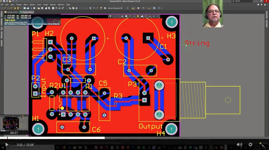
Schematic Capture with Altium: Best Practices
Efficient schematic capture is foundational to successful PCB design. Altium Designer offers a robust environment for creating clear and accurate schematics, which directly impacts the PCB layout and overall project success. This section delves into techniques for optimizing schematic design within Altium, focusing on component placement, wiring, and library management to ensure a smooth transition to PCB layout.
The following best practices aim to streamline the schematic capture process:
- Strategic Component Placement:
Organize components logically, grouping related components together. This mirrors the flow of the circuit and aids in visual clarity, making error detection easier during both design and review. Keep input and output sections distinct to enhance circuit readability. - Effective Wiring Techniques:
Use a consistent approach for wiring, like utilizing bus lines for parallel signals and avoiding excessive wire crossings. Altium’s Smart Wiring tools can significantly expedite the process and ensure connections are accurately made, reducing the potential for errors. Use net labels to clarify signal paths, especially across larger schematics. - Library Management:
Maintain well-organized libraries with up-to-date component information (symbol, footprint, and parameters) to ensure data consistency throughout the design. Altium provides cloud-based and local component management capabilities. Consistent use of parameters, such as manufacturer part numbers, and datasheets linked directly to component ensures traceability and reduces the likelihood of errors during procurement. - Hierarchical Design:
Use hierarchical design methodologies by dividing large complex projects into smaller, manageable blocks. This improves design organization, reuse of schematic elements and simplifies the overall design and review process. Altium's ability to support multi-channel design is particularly useful for handling repeated circuits in large designs. - Use Design Rules and Checks:
Regularly use Altium’s error checking features, like the Electrical Rule Check (ERC), to catch design issues early in the schematic capture phase. These checks help identify wiring errors, component misconnections, and missing component parameters, significantly minimizing errors before moving to the PCB layout stage.
Advanced PCB Layout Techniques in Altium
Effective PCB layout is crucial for ensuring the functionality and reliability of electronic devices. Altium Designer provides a comprehensive suite of tools for managing complex layouts, including layer management, sophisticated routing strategies, and component placement techniques that prioritize signal integrity and manufacturability. These advanced techniques are essential for achieving optimal performance and reducing manufacturing costs.
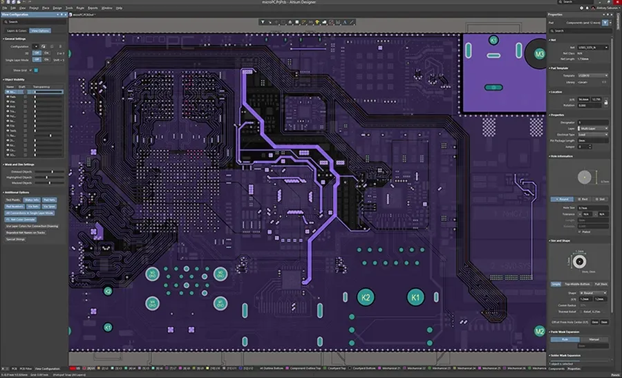
- Layer Management
Proper layer stack-up is fundamental for signal integrity and impedance control. Altium allows you to define your layer stack with precision, including dielectric materials and thickness, which is crucial for creating high-speed designs. Consider using dedicated layers for ground and power planes to minimize noise and ensure efficient power delivery. - Routing Strategies
Employ differential routing for high-speed signals to minimize noise and improve signal integrity. Utilize length matching techniques for critical signals to ensure synchronization. Keep sensitive analog traces away from digital ones to reduce cross-talk, and employ a grid-based approach for consistent track placement. - Component Placement
Careful component placement is necessary to minimize routing complexity and potential signal integrity issues. Group similar components together, place bypass capacitors close to power pins, and orient high-frequency components to minimize trace length. Consider thermal management requirements when placing high power dissipating components. - Impedance Control
Altium allows you to define impedance profiles for your board. Use these tools to match the impedance of your traces to the characteristic impedance of the components, which is vital for minimizing signal reflections and ensuring optimal signal transmission. Use impedance calculators to determine appropriate trace widths and spacing for your design parameters. - Power Delivery
Effective power delivery requires careful attention to plane design and decoupling capacitor placement. Employ wider traces or planes for power nets to minimize voltage drop. Place decoupling capacitors close to the power pins of ICs to minimize transient noise and reduce inductance. Consider the current carrying capacity for power traces to prevent overheating.
| Technique | Description | Benefits |
|---|---|---|
| Layer Stack-Up Design | Defines the structure of the PCB including dielectric materials and thickness. | Optimized impedance control and signal integrity. |
| Differential Routing | Routing signals as matched pairs with equal length and spacing. | Improved noise immunity and reduced electromagnetic interference. |
| Length Matching | Adjusting trace lengths to ensure signals arrive simultaneously. | Synchronization of signals and reduced timing issues. |
| Bypass Capacitor Placement | Placing capacitors close to power pins of components. | Reduced voltage spikes and improved power stability. |
| Impedance Matching | Adjusting trace dimensions to match impedance with components and source | Minimizes signal reflections and ensures signal integrity. |
Utilizing Altium's 3D PCB Visualization
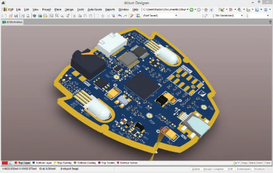
Altium's 3D PCB visualization feature provides an invaluable tool for designers to inspect their boards in a realistic, three-dimensional environment, going beyond traditional 2D layouts. This capability is essential for identifying potential mechanical interferences, optimizing component placement for accessibility and thermal performance, and ensuring the design aligns perfectly with its intended enclosure. By offering a comprehensive view of the assembled board, 3D visualization streamlines the design validation process, minimizing the risk of costly rework and accelerating the product development timeline.
- Mechanical Clash Detection
3D visualization allows designers to identify and resolve potential mechanical clashes between components, the PCB, and the enclosure before manufacturing. This avoids costly rework. - Component Placement Optimization
Engineers can visually assess the accessibility of components for assembly and testing, optimizing placement for ease of manufacturing and reducing potential interference issues. - Thermal Management Assessment
Visualizing the PCB in 3D helps in understanding the thermal profile by allowing better placement of components that generate more heat and ensuring adequate space for heat dissipation. - Realistic Simulations
The 3D view provides a better understanding of the final product, which allows for a more realistic simulation of the board's performance within its intended environment. This helps identify issues early in the design process. - Improved Design Communication
3D visualizations enhance communication among design, manufacturing, and mechanical teams, ensuring everyone has a clear understanding of the design’s physical characteristics.
| Feature | Benefit |
|---|---|
| 3D Viewing | Provides realistic view of the assembled board |
| Clash Detection | Identifies potential mechanical conflicts early |
| Placement Visualization | Optimizes component layout for functionality and manufacturability |
| Thermal Analysis Aid | Supports strategic component placement for effective thermal management |
| Enhanced Communication | Ensures clear communication across various engineering teams |
| Reduced Rework | Minimizes the risk of post-production issues by pre-emptive validation |
Signal Integrity Analysis and Simulation in Altium
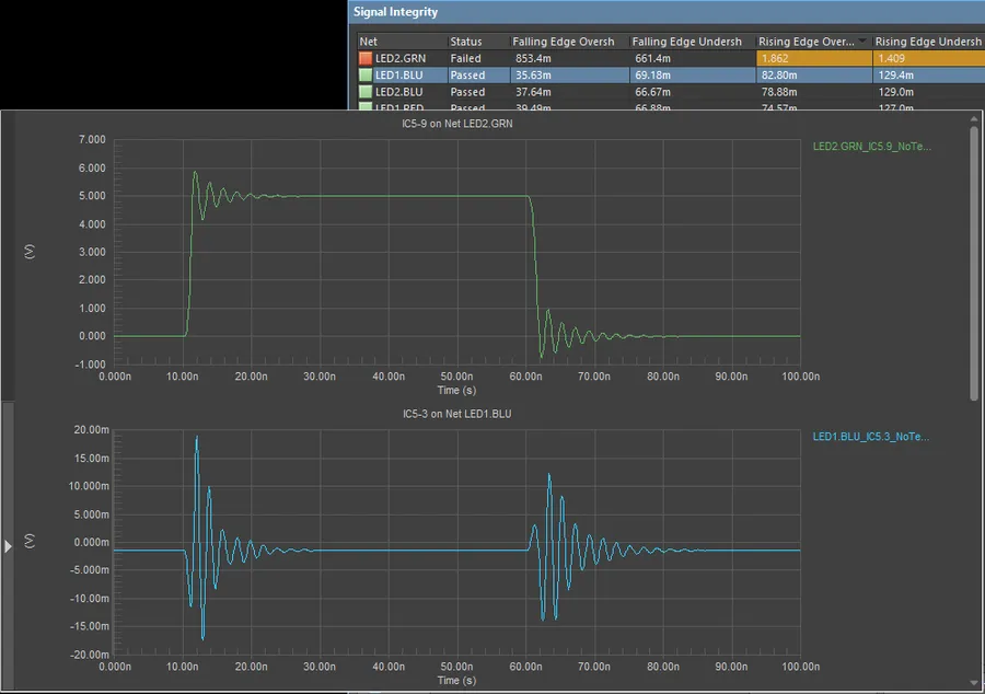
Signal integrity (SI) analysis and simulation within Altium Designer are critical for ensuring that PCB designs function reliably, particularly at high speeds. By proactively identifying and rectifying potential signal issues during the design phase, engineers can avoid costly redesigns and ensure robust performance of their electronic products. Altium Designer offers a suite of tools to simulate, analyze, and optimize signal behavior, encompassing impedance control, reflection management, crosstalk mitigation, and power distribution network (PDN) analysis.
- Impedance Control
Altium's field solver allows accurate calculation of characteristic impedance for various trace geometries, which is crucial for matching impedances to minimize signal reflections. - Reflection Analysis
Simulate signal reflections arising from impedance mismatches along signal paths. This ensures that signals are not corrupted by reflections, which can cause data errors and instability. - Crosstalk Analysis
Evaluate the coupling of signals between adjacent traces, a critical consideration in high-density designs. Tools identify locations where crosstalk might lead to interference and suggest spacing modifications or shielding techniques. - Power Distribution Network (PDN) Analysis
Assess the PDN impedance to ensure it is sufficiently low to prevent voltage fluctuations that can compromise device performance. This analysis involves considering capacitance, inductance, and resistance at various frequencies within the PDN. - Time-Domain Reflectometry (TDR) Simulation
Simulate the propagation of signals along transmission lines in the time domain to observe reflections and signal distortions directly. This is a key technique for diagnosing signal integrity issues. - Frequency-Domain Analysis
Analyze the behavior of signals across a wide frequency range, which helps uncover frequency-specific issues, such as resonance in the PDN or poor filter performance. - Pre and Post Layout Simulation Capabilities
Altium provides pre-layout and post-layout simulation capabilities that enable the designer to simulate designs early in the design process or accurately analyze results after layout is complete. This approach allows for early detection of issues and rapid iterative improvement
| Analysis Type | Purpose | Key Parameters Analyzed |
|---|---|---|
| Impedance Analysis | Ensure controlled impedance to minimize signal reflections | Characteristic impedance, trace dimensions, stack-up properties |
| Reflection Analysis | Identify signal reflections due to impedance mismatches | Reflection coefficient, transmission line termination, impedance discontinuities |
| Crosstalk Analysis | Evaluate the coupling of signals between adjacent traces | Coupling capacitance, coupling inductance, trace spacing |
| PDN Analysis | Assess the stability and integrity of the power delivery network | PDN impedance, DC voltage drop, current density, decoupling capacitor effectiveness |
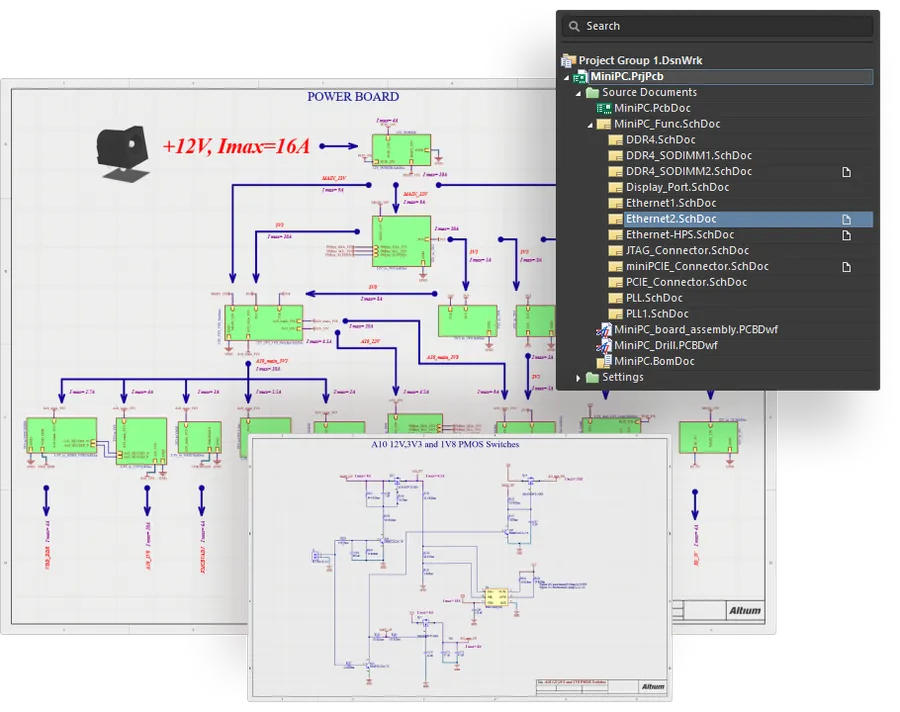
Collaborative Design Workflow with Altium 365
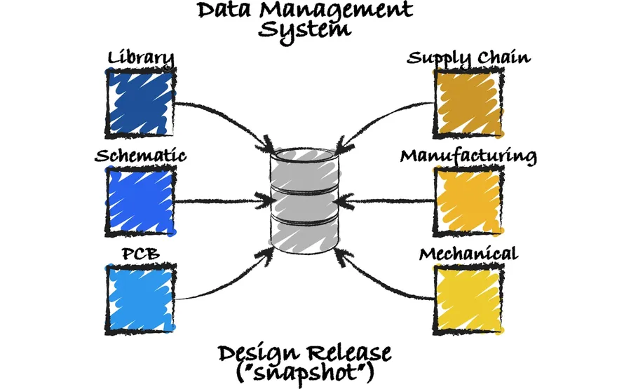
Altium 365 facilitates a robust collaborative PCB design environment, enabling seamless sharing, version control, and project management for teams. This cloud-based platform integrates directly with Altium Designer, providing a unified space for all design stakeholders to work concurrently and efficiently.
Key benefits of utilizing Altium 365 for team-based PCB design include:
- Concurrent Design Capabilities
Multiple designers can access and modify the same project simultaneously without overwriting changes or creating conflicts. This dramatically reduces design time. - Version Control
Altium 365 tracks changes to the project throughout its development history, making it easy to revert to previous versions or compare design iterations. Every modification is automatically recorded in a way that prevents data loss and gives users a complete timeline of changes. - Centralized Project Storage
The platform offers a secure, cloud-based repository for all project files, schematics, PCB layouts, and component libraries. Centralized storage eliminates the need for cumbersome local file sharing, thereby reducing the chance of losing files or using outdated information. - Real-Time Review and Feedback
Designers can share their work with stakeholders in real time, enabling immediate reviews and feedback. This streamlined review process facilitates faster iteration and allows for a better design. - Improved Project Management
Altium 365 provides features that help project management including status updates, user permissions, and comments, which make it easier to track project progress and keep stakeholders updated. This helps manage project milestones and keep the whole team on target.
To maximize the effectiveness of Altium 365 for collaborative workflows, consider the following:
- Establish Clear Communication Channels
Define communication channels within your team to ensure everyone is aware of changes and deadlines. - Utilize Roles and Permissions
Use Altium 365's roles and permissions system to control who has access to which parts of the design and what they can change. - Regularly Backup Designs
Although Altium 365 provides version control, it's still important to set up processes to regularly backup designs, adding an extra layer of safety. - Train the Team
Ensure all members of the team are well versed in using Altium 365's collaboration tools and features. Training should include best practices for sharing data, commenting, and managing project changes.
Frequently Asked Questions About Altium PCB Design
This section addresses common queries regarding Altium PCB design, covering aspects from cost and licensing to functionality and software comparisons. It aims to provide clear, concise answers to help users understand Altium's capabilities and suitability for their PCB design needs.
- Is Altium Designer free to use?
Altium Designer is not free. It is a professional-grade software that requires a paid license. However, Altium offers a free trial version for evaluation and educational purposes. There is also a student license available for eligible individuals. It's crucial to note that while trial versions and student licenses provide access to the full software suite, they might come with limitations, such as commercial use restrictions or certain feature limitations. - What are the primary applications of Altium Designer?
Altium Designer is primarily used for designing printed circuit boards (PCBs) and electronic products. Its applications span across various industries, including consumer electronics, aerospace, automotive, and medical devices. Altium provides a comprehensive suite of tools for schematic capture, PCB layout, signal integrity analysis, and more, making it a versatile solution for complex electronic design projects. Moreover, its integration with mechanical CAD software allows for complete product design. - How much does Altium Designer cost?
The cost of Altium Designer varies depending on the type of license and subscription model chosen. Altium offers various license options, including perpetual licenses and time-based subscriptions. Furthermore, specific regional variations in pricing may exist. The exact cost is best obtained by directly contacting Altium sales or its authorized resellers, as pricing models are subject to change. It is also worth noting that Altium 365, the cloud-based collaboration platform, is typically an additional cost beyond the basic Altium Designer license. - What PCB design software is considered the best alternative to Altium Designer?
While the "best" software is subjective to an individual's specific needs and requirements, some popular alternatives to Altium Designer include Cadence Allegro, Mentor Xpedition, and KiCad. Each has its strengths; Cadence and Mentor are often chosen for very complex designs at high-end applications, while KiCad is a completely free and open source solution. The choice of software often depends on factors such as project budget, design complexity, user expertise, and specific industry standards and regulatory compliance. - Is there an Altium student license available?
Yes, Altium offers a student license for eligible students at accredited educational institutions. This student license is typically offered for free or at a reduced cost to facilitate academic learning and research. However, student licenses typically have specific restrictions, including non-commercial use limitations and limited availability of technical support. Eligibility criteria must be met by individual students to obtain a student license. - How does Altium handle collaborative design processes?
Altium excels in collaborative design through its Altium 365 platform, which provides a cloud-based environment for team collaboration. Key features include project sharing, version control, and real-time commenting. This collaborative system allows multiple users to concurrently work on the same project, streamline workflows and enhance team productivity. Altium 365 integrates smoothly with Altium Designer to provide a comprehensive collaborative design ecosystem. - Can Altium be used to simulate the signal integrity of a PCB design?
Yes, Altium Designer has built-in tools for signal integrity analysis and simulation. These tools are essential for high-speed designs to identify and resolve potential signal issues, such as reflections, crosstalk, and impedance mismatches. The simulations help to ensure that the circuit performs as designed before fabrication. This analysis involves parameters like characteristic impedance, delay, and coupling coefficients, all critical for high-performance PCB designs.
Integrating Altium with Manufacturing Processes
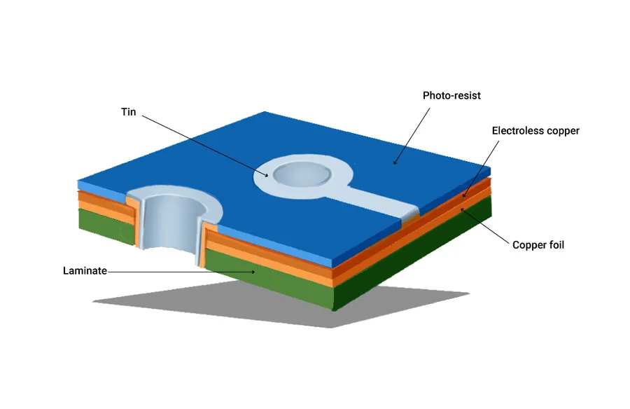
Successfully transitioning an Altium PCB design from the digital realm to a physical product requires meticulous preparation for manufacturing. This section provides a comprehensive overview of how to effectively integrate your Altium design with manufacturing processes, focusing on design file preparation, partner selection, and Design for Manufacturing (DFM) best practices.
Key aspects of integration include generating accurate manufacturing files (such as Gerber, ODB++, and NC drill files), adhering to DFM guidelines to minimize production issues, and establishing a clear communication channel with your chosen manufacturing partner. Understanding these aspects ensures a smooth and cost-effective transition from design to production.
| Manufacturing Step | Altium Action | Considerations |
|---|---|---|
| File Generation | Configure Output Jobs to generate Gerber, ODB++, and NC Drill files | Verify file formats, layers, and units to ensure compatibility with the manufacturer's requirements. |
| Design Rule Checks (DRC) | Run thorough DRC in Altium to detect potential manufacturing issues. | Address any violations and ensure that the final design meets manufacturability standards. |
| Bill of Materials (BOM) Preparation | Generate a complete and accurate BOM | Include all necessary component details, such as manufacturer part number and footprints. |
| Component Placement | Optimize component placement and orientation for automated assembly. | Consider reflow profile, component clearance, and testability aspects. |
| Panelization (If Required) | Utilize Altium's panelization tools, when required. | Ensure that panel size, spacing and fiducial placement align with manufacturing capabilities. |
| Communication with Manufacturer | Share design files, BOM, and manufacturing specifications with the chosen manufacturer. | Clarify any technical questions, material specifications or special requirements prior to production. |
Selecting the right manufacturing partner is crucial. Factors to consider include their experience with similar projects, technology capabilities, turnaround times, certifications, and cost. Establishing clear communication channels helps to address queries efficiently and ensures a successful production run, minimizing errors and delays. DFM implementation at the early stages of PCB design significantly reduces manufacturing issues, cost and production time.
Tips and Tricks for Efficient Altium PCB Design
Efficient PCB design in Altium involves leveraging its powerful features and adopting streamlined workflows. This section focuses on practical tips and tricks to boost your productivity, encompassing keyboard shortcuts, automation strategies, and community resources for optimized PCB development.
- Master Keyboard Shortcuts
Familiarizing yourself with Altium's extensive library of keyboard shortcuts can drastically reduce design time. Commonly used shortcuts include those for zooming, panning, selecting, and placing components, and learning these will minimize reliance on menus and toolbars. - Utilize Customization Options
Tailor Altium’s environment to match your specific workflow by creating custom panels, toolbars, and shortcuts that cater to your project requirements. This can lead to a more personalized and efficient design process. - Leverage Automation Scripts
Altium supports scripts (e.g., via Altium's Scripting system or Python scripting) to automate repetitive tasks, such as component placement, net naming, and report generation. Investing time to set up automation scripts will provide long-term time savings. - Effective Library Management
Maintain well-organized and up-to-date component libraries. Using a robust component library system saves time and prevents errors by ensuring consistency across designs. Additionally, using Altium's Managed Components features provides lifecycle and supply chain information. - Smart Component Placement
Utilize Altium's component placement tools effectively. Group related components, use the auto-placement features as a starting point, and consider thermal and signal integrity requirements during component placement. - Efficient Routing Strategies
Employ Altium’s powerful routing tools to reduce the time and complexity of your PCB routing. Utilize differential pair routing, interactive routing, and auto-routing features (with caution) where appropriate. - Community Resources and Forums
Tap into the vast Altium community for support, tutorials, and design tips. Forums and online resources can be invaluable when troubleshooting issues or discovering new techniques.
Altium PCB provides comprehensive solutions for every phase of PCB design, from schematic capture to fabrication. Whether you are working on simple or complex designs, mastering Altium PCB will greatly enhance your workflow and ensure high-quality end products. By embracing its collaborative features and advanced analysis tools, users can design high-performance electronic devices more efficiently.