Mastering Altium PCB Design: A Comprehensive Guide
In today's rapidly evolving tech landscape, the demand for high-quality and efficient printed circuit board (PCB) designs is paramount. Altium Designer, a leading PCB design software, empowers engineers to transform their ideas into reality. This guide serves as your gateway to mastering Altium PCB design, exploring its functionalities, best practices, and offering practical insights to create top-tier PCBs.
Setting Up Your Altium Designer Environment
Establishing a well-organized Altium Designer environment is crucial for efficient and effective PCB design. This involves creating new projects, managing files, configuring the workspace, and customizing settings to match design needs and workflow preferences, ultimately contributing to an optimal design experience.
- Project Creation
Initiate a new project using the 'File' > 'New' > 'Project' command, selecting the appropriate project type (e.g., PCB Project, Integrated Project) based on your design requirements. A new project will create the folder structure and project file required to begin the design process. - File Management
Employ clear and consistent naming conventions for project files, ensuring all project-related data, including schematics, PCB layouts, and libraries, is logically organized and stored within the designated project folder to maintain file integrity and ease of access. - Workspace Configuration
Configure the Altium Designer workspace by customizing the panels, toolbars, and shortcuts to create a personalized design environment that best suits your needs. This can include docking specific panels in easily accessible areas or creating new panels for frequently used functions. - Preference Customization
Personalize software settings through the 'DXP' > 'Preferences' menu, focusing on aspects such as visual theme, units of measure, and design rule settings. Tailoring these settings to your workflow enhances both efficiency and design precision.
Schematic Capture: Building the Foundation
Schematic capture in Altium Designer is the crucial first step in PCB design, serving as the blueprint for your physical board. It involves creating a logical representation of your circuit using symbols and connections, establishing the foundation for the subsequent PCB layout process. Mastering this step ensures accurate and efficient board development.
- Component Placement
Start by placing electronic components (resistors, capacitors, ICs, etc.) onto your schematic sheet. Altium's library management is essential here, allowing access to a vast array of pre-built components. - Wiring and Connections
Use net labels and wires to create connections between component pins. Ensure all connections are logically consistent with your circuit design. Double check for floating pins and unintended shorts. - Library Management
Efficiently manage component libraries, including both built-in and custom components. Maintain up-to-date component information to avoid supply chain issues. Create or modify part symbols as needed to meet your unique design needs. - Custom Part Creation
Develop custom parts by defining symbols, footprints, and parametric information. This process is necessary for components that are not available in standard libraries. Proper custom part creation ensures accurate part representation throughout the design process, helping with material selection later on. - Annotation and Validation
Annotate your schematic to ensure clarity and ease of understanding, with clear designators, values, and net names. Always validate your schematic using Altium's built-in checks to identify and correct errors before moving forward.
| Aspect | Description |
|---|---|
| Component Libraries | Altium provides an extensive library of standard components, but also allows for custom additions. Proper library management is critical for design accuracy and efficiency. |
| Net Labels | Net labels are used to define electrical connections between component pins and sections of the circuit. They improve clarity, especially in complex schematics. |
| Component Parameters | Each component can have specific parameters that include information such as manufacturer part number, footprint type, tolerances, and temperature ratings. Using component parameters ensures proper part selection and accurate bill of materials generation. |
| Schematic Validation | Altium offers a range of checks to ensure schematic accuracy. This includes validation of electrical connectivity, correct symbol association to part selection, and annotation completeness. Running these checks before moving on can avoid later errors. |
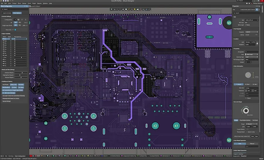
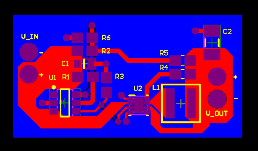
PCB Layout: Transforming Schematic to Physical Board
The PCB layout process in Altium Designer is the crucial step where the logical design captured in the schematic is translated into a physical board. This involves importing the schematic, defining the board's structure, strategically placing components, routing traces for electrical connections, and applying design rules to ensure functionality and manufacturability.
- Importing the Schematic
The first step is to import the completed schematic design into the PCB editor. Altium intelligently transfers all component and net information, laying the foundation for your physical layout. This ensures that the logical design is accurately translated into the physical board. - Setting up Layers
Configure the layer stack according to your design's complexity and manufacturing requirements. Assign specific layers for signals, power, ground, and silkscreen. Proper layer management is essential for signal integrity and manufacturing. - Defining Board Shape
Define the physical outline of your PCB, considering space constraints and the mechanical enclosure. Accurate board shapes are crucial for proper fit and avoiding mechanical interference. - Component Placement
Strategically place components on the board, considering signal paths, thermal constraints, and design rules. Optimization of component placement can significantly impact the performance and routability of the PCB. - Routing Traces
Connect components by routing traces according to the schematic netlist. Use Altium's routing tools to create clean and efficient paths, adhering to impedance requirements and design rules. - Applying Design Rules
Set up and enforce design rules to ensure the PCB meets electrical, mechanical, and manufacturing standards. This includes clearance rules, trace width specifications, and via size requirements. Design rules are critical for preventing manufacturing defects and ensuring the PCB's reliability.
| Aspect | Description | Considerations |
|---|---|---|
| Schematic Import | Transfers component and net data | Ensure schematic is finalized and error-free |
| Layer Stack | Configuration of PCB layers | Signal, power, ground, and fabrication needs |
| Board Outline | Physical shape of the PCB | Mechanical fit and enclosure requirements |
| Component Placement | Positioning of components | Signal flow, thermal management, and routing |
| Routing | Connecting components via traces | Impedance control, signal integrity, and trace width |
| Design Rules | Manufacturing and electrical parameters | Clearances, trace widths, and via sizes |
Advanced Routing Techniques in Altium
Mastering advanced routing techniques in Altium Designer is crucial for creating high-performance PCBs. This section delves into differential pair routing, controlled impedance routing, and via-in-pad (VIP) technology, essential for robust and high-speed designs.
| Technique | Description | Applications | Altium Implementation |
|---|---|---|---|
| Differential Pair Routing | Routing two traces with equal length, impedance, and spacing for noise reduction. | High-speed data interfaces (USB, Ethernet, PCIe). | Use Altium's Interactive Differential Pair Routing tool. Set specific spacing and impedance targets. |
| Controlled Impedance Routing | Routing traces with specific impedance to minimize signal reflections. | RF and high-speed digital signals. | Define impedance profiles in Altium's layer stack manager. Calculate trace width and spacing to achieve the desired impedance. Utilize impedance calculators. |
| Via-in-Pad (VIP) Technology | Placing vias directly within the component pads to reduce inductance and size. | High-density BGA and fine-pitch components. | Use Altium’s via stitching with specific settings. Ensure proper manufacturing capabilities and rules are set. |
- Differential Pair Routing Considerations
Ensure equal trace lengths for time-aligned signals. Maintain consistent spacing to control differential impedance. Use Altium's interactive routing tool for precise control. - Controlled Impedance Guidelines
Calculate impedance using Altium's impedance calculator, considering layer stack properties. Adjust trace width and spacing to meet impedance requirements. Verify impedance with Altium's simulation tools. - Via-in-Pad Design Rules
Confirm manufacturing capabilities for plated vias in pads. Ensure adequate copper fill for thermal and electrical connections. Use appropriate via sizes to avoid solderability issues.
Power Integrity and Signal Integrity Considerations
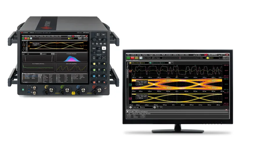
Power Integrity (PI) and Signal Integrity (SI) are crucial aspects of PCB design that significantly impact the reliability and performance of electronic devices. Power integrity ensures a stable and clean power delivery network, while signal integrity focuses on maintaining signal quality during transmission. Addressing both is paramount for achieving successful PCB functionality, especially in high-speed and high-frequency applications. Neglecting these considerations can lead to signal distortion, timing errors, and even complete system failures, thus making their effective management an essential skill for any Altium PCB designer.
- Power Integrity (PI)
Ensures the stable and clean delivery of power to all components on the PCB. Issues include voltage drops, noise, and impedance mismatches. A stable power supply is critical for optimal component performance and system reliability. - Signal Integrity (SI)
Maintains the quality of electrical signals during transmission. Concerns include signal reflections, crosstalk, and electromagnetic interference (EMI), which can degrade signal quality and cause data errors or system malfunction. High-speed signals are particularly susceptible to these issues.
| Issue | Description | Altium Mitigation Tools |
|---|---|---|
| Voltage Drop | Reduction in voltage level from source to load, especially during high current draws. | DC analysis, power plane design tools |
| Ground Bounce | Fluctuations in the ground potential, impacting reference for signal levels. | Ground plane optimization, decoupling capacitors |
| Signal Reflections | Signals bouncing back due to impedance mismatch. | Impedance matching tools, trace routing strategies |
| Crosstalk | Unwanted signal coupling between adjacent traces. | Spacing rules, differential routing |
| EMI/EMC | Electromagnetic Interference that can affect circuit behavior or be radiated externally. | Shielding layers, filtering components |
Altium Designer provides a suite of analysis tools to mitigate PI and SI issues, including reflection analysis and impedance calculation. These tools enable designers to identify potential problems early in the design process, allowing for necessary adjustments to the layout before fabrication. Proper use of these tools is crucial for creating reliable and high-performance PCBs. Decoupling capacitor placement, power and ground plane design, and trace impedance matching are essential techniques to ensure that power and signals are distributed effectively across the board.
Utilizing Altium's 3D PCB Capabilities
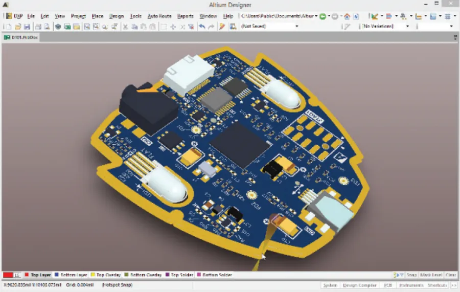
Altium Designer's 3D PCB capabilities provide a powerful tool for visualizing and verifying your designs, moving beyond traditional 2D layouts to offer a realistic representation of the assembled board. This functionality is crucial for detecting mechanical interferences, ensuring component clearances, and validating the overall fit of your design within its intended enclosure.
- Enhanced Design Visualization
The 3D view allows designers to see a realistic representation of the PCB, facilitating better understanding of component placement and potential mechanical issues. This aids in identifying problems that may not be apparent in a 2D layout, such as component collisions or conflicts with the enclosure. - Mechanical Interference Detection
By visualizing the board in 3D, designers can easily detect mechanical interferences, such as components colliding with each other or with the enclosure. This is crucial for ensuring that the assembled board will fit and function correctly. - Clearance Verification
The 3D view provides the ability to check for proper clearance between components and the enclosure or other parts of the design. This is critical to avoid short circuits or mechanical damage during assembly or operation. - Accurate Assembly and Fit Validation
3D visualization permits a thorough validation of the assembly process. You can examine the board from all angles to determine accessibility for automated or manual assembly, including correct part placement and orientations. - Enhanced Collaboration
Altium’s 3D view facilitates better communication between electrical and mechanical engineers, as it provides a common platform to discuss the design, visualize assembly processes, and identify potential problems.
| Feature | Benefit |
|---|---|
| 3D Viewing | Offers realistic visualization of the assembled PCB. |
| Interference Check | Detects mechanical clashes between components and enclosures. |
| Clearance Analysis | Ensures adequate spacing between components to avoid electrical and mechanical issues. |
| Assembly Verification | Validates the assembly process for accuracy and efficiency. |
| Collaboration Tool | Enhances communication between electrical and mechanical design teams. |
Generating Manufacturing Files (Gerber, ODB++)
The culmination of PCB design in Altium involves the precise generation of manufacturing files, primarily Gerber, ODB++, drill, and pick-and-place files. These files are the blueprint for fabricating and assembling your designed circuit board. Understanding the nuances of these file formats and how to generate them correctly using Altium is critical to ensuring a smooth transition from design to production.
Gerber files are the most common standard for PCB manufacturing, representing each layer of your board as a separate file. ODB++ is a more comprehensive format that encapsulates all design data into a single file, including layer information, component details, and netlist information. Drill files specify hole locations, while pick-and-place files provide the coordinates and rotation of components required for automated assembly. Generating these files correctly is essential to avoid manufacturing issues.
| File Type | Description | Content | Usage |
|---|---|---|---|
| Gerber (RS-274X) | Industry-standard format for PCB layer information. | Vector data representing copper, solder mask, and silkscreen layers. | Used by PCB manufacturers to fabricate the bare board. |
| ODB++ | Intelligent, comprehensive format containing all design data. | Layer information, component data, netlist. | Used by manufacturers for fabrication and assembly; facilitates DFM analysis. |
| Drill Files | Specifies the locations and sizes of drilled holes. | X,Y coordinates and drill diameters. | Required for drilling operations during fabrication. |
| Pick-and-Place Files | Provides component placement data for assembly machines. | Component reference, X,Y coordinates, rotation, and layer. | Used by automated assembly equipment to place components onto the PCB. |
- Configure Output Job File:
In Altium, output job files manage the generation of manufacturing data. Configure it to include necessary output types (Gerber, ODB++, drill, pick and place). - Set up Gerber Output:
Select the appropriate Gerber format (RS-274X is most common) and configure layer selection, units, and precision. - Configure ODB++ Output (Optional):
If your manufacturer uses ODB++, configure the output parameters to generate a complete dataset. - Generate Drill Files:
Specify drill file format and units (e.g. Excellon) to generate drill data. - Generate Pick-and-Place Files:
Set up the output format and select the desired components, including reference designator, X,Y coordinates, rotation, and layer. - Verification:
Always review generated files using a gerber viewer to catch potential errors before sending data to production.
Frequently Asked Questions About Altium PCB Design
This section addresses common queries encountered while using Altium for PCB design. These questions and their comprehensive answers are designed to clarify typical confusions and provide practical guidance.
- How do I create a custom component footprint in Altium?
To create a custom component footprint, start by opening the PCB library editor. Utilize the various drawing tools to construct the pads, silkscreen, and other necessary elements. Ensure your design adheres to the component's datasheet specifications. After completing the footprint, save it within your library, making it accessible for future projects. - What are the recommended system requirements for running Altium Designer effectively?
Altium Designer performs optimally with a robust system. At a minimum, it requires a 64-bit Windows operating system, an Intel Core i5 processor (or equivalent), 8 GB of RAM (16 GB or more is recommended for large designs), and a dedicated graphics card supporting DirectX 10 or higher. Solid State Drive (SSD) is strongly recommended for faster performance. Regularly check Altium's official website for the most up-to-date system recommendations as software updates frequently introduce changes. - How can I perform basic simulations and signal analysis in Altium?
Altium Designer provides basic signal integrity analysis tools. To perform basic simulations, use the 'Simulate' menu option after the schematic is designed. You may need to specify the required component parameters or models. Ensure to configure the simulation options correctly to accurately represent the performance characteristics of your design. For more comprehensive simulations, specialized third-party tools can be used. - Is Altium Designer free for students?
Altium offers a student license, often at a reduced cost, with specific conditions. It's crucial to check the official Altium website for details on eligibility, the licensing process, and the terms of use. The student license is generally intended for educational purposes and may not be utilized for commercial projects. - How long does it typically take to learn Altium for PCB design?
The learning curve for Altium varies. Basic proficiency for simple PCB designs can be acquired in a few weeks with focused study and practice. Mastering advanced features and complex designs may take several months to a year, depending on individual dedication and experience. Regularly practicing and working on real-world projects is key to gaining expertise. - What file formats does Altium use to generate manufacturing files?
Altium primarily uses Gerber (RS-274X or X2) format for PCB manufacturing, drill files in Excellon format, pick-and-place files usually in CSV or TXT format, and optionally ODB++ format. Gerber files describe the copper layers, solder mask, and silkscreen layers, while drill files specify drilling locations, and pick-and-place files list the component location and orientation for automated assembly. Always ensure the output settings match the manufacturer's requirements. - What are the best practices for managing PCB design files in Altium?
To manage PCB design files effectively, adopt a systematic approach. Use a version control system (such as Git) to track changes. Create clear file-naming conventions. Regularly back up project files on both local and cloud storage and adhere to a consistent folder structure. Use Altium’s project packager to archive the entire project, including all libraries and output files, to ensure easy sharing and archiving for future access and modification. Also, use project variants to track multiple designs.
Optimizing Your Workflow in Altium Designer
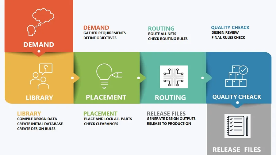
Efficient workflow in Altium Designer is crucial for minimizing design time and maximizing productivity. This section outlines key strategies for project management, effective collaboration, and leveraging automation to streamline your PCB design process.
- Project Management Best Practices
Establishing a well-organized project structure is foundational for smooth design iterations. Utilizing version control systems (like Git) and maintaining clear naming conventions for components, schematics, and PCB files are essential. Consistently backup your project files to prevent data loss, especially during critical design phases. - Component Library Management
Use Altium's managed component library features to ensure part consistency and availability. Regularly update and verify the accuracy of your library components. Establish a robust process for adding new parts. Avoid manually creating components and instead reuse existing ones. You can also use Altium Vault to create and manage a company library. - Effective Collaboration Techniques
Utilize Altium 365 for collaborative design, allowing multiple engineers to work on a project concurrently and view changes in real time. Clearly define roles and responsibilities within the team. Use comment and markup tools to provide feedback and communicate design changes effectively. Version control is critical for multi-user collaboration and design tracking. - Leveraging Automation Features
Take advantage of Altium's automation capabilities, such as design rule checks (DRCs), autorouting, and scripting. Master the use of variant management to avoid repetitive tasks in multi-variant projects. Automate report generation for BOMs, assembly drawings, and other documentation. Consider Altium’s scripting engine for unique tasks. - Customizing your Altium Environment
Tailor your environment to your specific needs by configuring keyboard shortcuts, customizing the ribbon, and setting up workspace preferences. Create and use templates to streamline project creation and setup. Regularly update your Altium software and check for updates that improve design workflow. - Design Rule Checks (DRC)
Implement and strictly adhere to robust DRC profiles for your project. Review and update DRC profiles for every new project. By continuously checking for design rule violations, costly manufacturing errors can be prevented. Be sure to customize your rule profiles to match the specific requirements of each design.
Mastering Altium PCB design is not just about using software; it's about understanding the principles of circuit design and employing best practices. By leveraging Altium's features and applying the techniques discussed in this guide, you'll enhance your skills and develop sophisticated and functional PCBs for your projects and further your understanding of Altium PCB design.