Choosing the Right PCB Design Company: A Comprehensive Guide
In today's tech-driven world, printed circuit boards (PCBs) are the backbone of nearly every electronic device. Choosing the right PCB design company is crucial for bringing your ideas to life. This guide from a seasoned PCB design company expert will help you understand what to look for, ensuring a successful project from concept to production. We'll cut through the noise, providing clear, actionable advice you can use immediately. Let's unravel the critical steps to selecting the best partner for your PCB needs.
Understanding Your PCB Design Needs
Before engaging a PCB design company, a thorough evaluation of your project's specific requirements is paramount. This initial assessment, focusing on project complexity, budgetary constraints, and timeline expectations, lays the groundwork for a successful design process. Identifying the necessary technology and specific application requirements for your project allows a PCB design company to tailor their services effectively, ensuring a design that aligns with your objectives and specifications.
- Project Complexity
Determine the complexity of your PCB design, considering factors such as layer count, component density, signal integrity requirements, and the use of advanced technologies like high-speed interfaces or RF circuits. Complex designs often require specialized expertise and more advanced design tools. - Budgetary Constraints
Establish a realistic budget for your PCB design project. Consider that design costs can vary significantly based on complexity, the design company’s experience, and the tools they employ. Transparent pricing practices with a detailed cost breakdown are important to ensure that your budget can cover your project's needs. - Timeline Expectations
Define a realistic timeline for your project, including design, prototyping, and manufacturing. Ensure that the PCB design company you choose can accommodate your timeline requirements and is capable of delivering results within your schedule. - Technology and Application Requirements
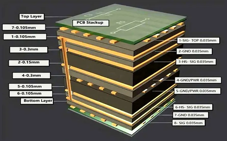
Identify the specific technologies required for your PCB, such as specific communication interfaces (e.g., USB, Ethernet, I2C, SPI), signal frequencies, power requirements, and environmental conditions. The application your PCB will be used for (e.g., medical, industrial, consumer) will also influence the design requirements and design constraints. These elements inform the company on which design guidelines must be met and which specializations are needed.
By clearly outlining your PCB design needs in these key areas, you set the stage for effective communication with potential PCB design companies. This detailed preparation ensures that you find a partner capable of delivering a high-quality, functional, and cost-effective PCB design.
Essential Services Offered by PCB Design Companies
PCB design companies provide a variety of crucial services that span the entire development lifecycle of a printed circuit board, from initial concept to final production. Understanding these services is critical to choosing a partner that meets your project's specific needs.
- Schematic Capture
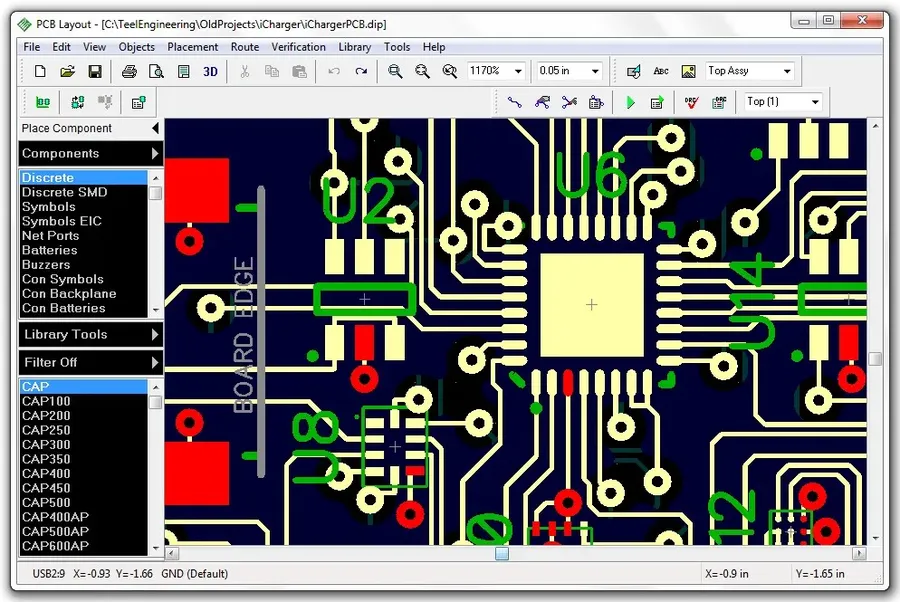
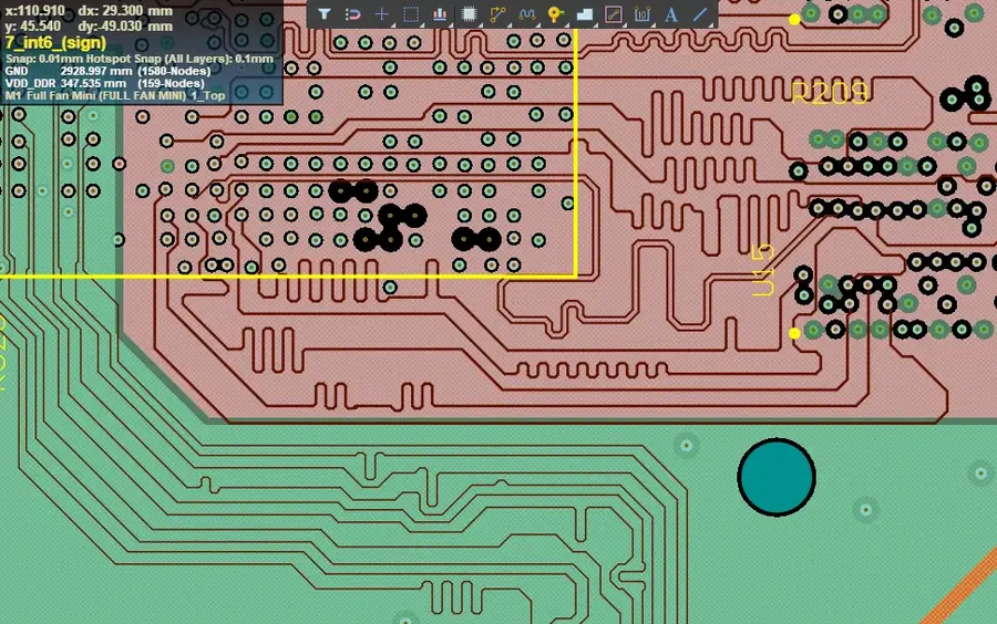
This foundational step involves creating a digital representation of the electronic circuit. It defines the components and their interconnections, forming the blueprint for the physical layout. Companies use specialized software to generate schematics accurately. - PCB Layout Design
The layout process translates the schematic diagram into a physical design. It determines the placement of components, routing of conductive traces, and overall structure of the PCB. Expertise in signal integrity, thermal management, and manufacturing constraints are vital during this stage. - Prototyping
Prototyping involves creating a physical test version of the PCB. This enables design validation and testing of functionality, which reduces errors and saves costs on final production. Companies offer varying prototyping services depending on project needs. - Assembly
The assembly service includes the population of the PCB with electronic components. This can be manual or automated using pick and place machines. Precision and adherence to industry standards are crucial during assembly.
In addition to the core services, many companies provide additional essential services:
- Simulation and Testing
These services use software to verify the design's performance and identify potential issues early in the design process before manufacturing. This process ensures functionality and reliability of the final product. - Design for Manufacturability (DFM)
DFM analyzes the design for manufacturability, ensuring that the PCB can be produced efficiently and cost-effectively. DFM will help reduce production time and costs. - Design for Testability (DFT)
DFT focuses on designing PCBs that are easy to test. DFT is a critical aspect of ensuring that any errors can be quickly found and addressed during the manufacturing process.
Choosing a PCB design company that offers a comprehensive suite of services, including DFM and DFT, can streamline the entire product development lifecycle, leading to reduced costs, and a more efficient and robust design process.
Evaluating PCB Design Company Experience and Expertise

Selecting a PCB design company with demonstrable experience and expertise is crucial for project success. This involves scrutinizing their past work, industry alignment, and the depth of their technical knowledge to ensure they can handle your project's specific needs.
A thorough evaluation of a PCB design company’s experience and expertise should include:
- Industry Alignment
Prioritize companies with a history of projects in your sector or with similar technological demands. This ensures they understand industry-specific challenges and requirements. - Portfolio Review
Request a detailed portfolio showcasing a range of past PCB design projects. This allows you to assess the complexity and scope of designs they've successfully handled. - Client Testimonials and References
Seek out client testimonials or direct references to gain insight into their past project management, design quality, and communication practices. This will provide valuable context and insights into their professional reputation. - Technical Specialization
Confirm the company has specialized knowledge in the design of the technologies your project requires. This may include high-speed design, RF design, analog design, digital design or other specializations.
The following table provides a breakdown of key considerations when evaluating a PCB design company's experience and expertise:
| Evaluation Criteria | Description | Importance |
|---|---|---|
| Portfolio Analysis | Review past PCB designs for technical complexity, variety, and quality. | Essential. Shows the company's ability and range of experience. |
| Industry Experience | Verify experience in your specific industry or in projects with similar requirements. | Critical for understanding industry-specific challenges. |
| Client Feedback | Assess client testimonials and references to check their reliability and service quality. | Provides insight into their reputation and service quality. |
| Technical Expertise | Confirm expertise in the specific technologies and design needs of your project. | Vital for successful project execution. |
Checking Design Software and Technology
A PCB design company's proficiency with industry-standard CAD software is paramount for efficient and accurate design processes. Utilizing current tools and technologies not only optimizes design workflows, but also minimizes errors and accelerates development times.
Here's why verifying a company's software and technology is critical:
- Compatibility
Ensures seamless file exchange and collaboration if you're using specific software or have existing design assets. - Efficiency
Modern CAD software offers advanced features and automation that can reduce design time and improve accuracy. - Error Reduction
Advanced tools, such as simulation and analysis software, help identify and rectify potential issues before manufacturing, saving significant costs. - Access to Advanced Design Features
Up-to-date software often comes with new capabilities, allowing for more complex and optimized designs.
Key considerations regarding software and technology:
- Software Versions:
Inquire about the specific versions of CAD software they use. This is important for compatibility and file sharing, particularly for complex projects. - Design Rule Checks (DRC):
Confirm their software can handle complex DRC for different technologies. Proper DRC ensures manufacturing success and minimizes production issues. - Simulation and Analysis Tools:
Determine if the company utilizes tools for signal integrity analysis, thermal simulation and other crucial performance assessments. - Library Management:
Assess their component library management system, which will help ensure accurate and consistent part usage. - Continuous Training:
Verify that the design team stays up-to-date with the latest software features and best practices.
| Software Category | Example Software | Key Function |
|---|---|---|
| CAD Software | Altium Designer, Cadence Allegro, KiCad | PCB layout, schematic capture |
| Simulation Software | Ansys SIwave, CST Studio Suite | Signal integrity, thermal analysis |
| CAM Software | Gerber viewer, Ucam | Preparation for PCB manufacturing |
Cost, Budgeting and Pricing Structures

Understanding the cost structures of PCB design companies is crucial for effective budgeting and project management. A detailed analysis of pricing models and potential expenses, including design, manufacturing, and assembly, ensures transparency and a trustworthy partnership.
When engaging a PCB design company, it's essential to move beyond initial quotes and delve into the specifics of how costs are determined. This approach allows for a clear understanding of what you're paying for and provides a solid foundation for a successful project.
| Cost Factor | Description | Impact on Budget |
|---|---|---|
| Design Complexity | Complexity of the schematic and layout requirements | High impact on design cost and time. |
| Technology Requirements | Specific layer count, materials, and impedance control | Directly affects material costs and manufacturing processes. |
| Project Scope | Number of revisions and level of involvement required from design company | Increases overall project costs and time. |
| Turnaround Time | Expedited delivery can result in higher costs | Higher costs for quick turnaround. |
| Testing and Validation | Types of simulation and testing processes | Increases the cost of design and production. |
| Manufacturing and Assembly | Cost based on the quantity, assembly type and complexity of the PCB | A large part of the total project cost. |
Below is an exploration of common pricing structures used by PCB design companies. It's important to note that many companies may use a combination of these structures. You should discuss pricing specifics with your chosen partner.
- Fixed Price
A project-based fixed price can be useful when the full scope is well defined. This model allows for predictable budgeting as long as there are no scope modifications. However, the potential for higher initial quotes can exist to compensate for unknowns. - Hourly Rate
The hourly rate model is common for projects with variable scope or undefined requirements. This approach allows for flexibility but can make it difficult to predict the total cost if project parameters change frequently. - Per-Component Cost
Some companies may charge per component on the board. This pricing is usually based on design complexity and time. - Tiered Pricing
Pricing may vary depending on the services provided. A PCB design company may offer various design packages and these packages can vary in complexity and cost.
It is crucial to request a detailed breakdown of all costs. This can include, but is not limited to, the items listed below. Clear understanding of these individual costs allows for detailed budget tracking and ensures that there are no surprise expenses as the project proceeds:
- Schematic Capture
Cost for creating the electrical schematic from project specifications. - PCB Layout
Cost for the physical layout of the PCB, including component placement, and routing. - Prototyping
Cost for producing a prototype of the PCB to validate its design. - Simulation and Testing
Cost for simulation and test procedures to verify the design. - Design for Manufacturability (DFM)
Cost for optimizing the PCB layout to reduce manufacturing expenses. - Design for Testability (DFT)
Cost for the design elements required for efficient testing of the PCB - Materials and Components
Costs of all materials used in the PCB construction - Assembly
Cost for assembling components onto the manufactured PCB.
Timeline and Project Management
Effective timeline management and project oversight are paramount when partnering with a PCB design company. A company's ability to deliver designs within specified deadlines and budgets directly impacts the success of your overall project. Robust project management isn't just about meeting dates; it's about ensuring seamless communication, clear understanding of objectives, and proactive issue resolution.
Key aspects to evaluate include:
- Project Timeline:
Assess the company’s capability to provide realistic and detailed project timelines. A credible timeline will clearly outline key milestones from schematic capture to final testing and assembly. Inquire about their procedures for handling deviations or delays. - Project Management Workflow:
A transparent workflow is essential. The company should have clearly defined processes for every stage of the project. Transparency fosters trust and ensures that all parties are aligned with the project’s progress. - Communication Protocols:
Regular updates and communication are the cornerstones of effective project management. Understand the company's communication process, the frequency of reporting, and the channels used. A responsive and communicative company is a key asset. - Risk Management Strategies:
A proactive approach to identifying and mitigating risks is important. Discuss potential challenges and how the PCB design company plans to address them. Their planning should encompass potential design hurdles and material sourcing. - Change Management:
Projects often require changes or adjustments along the way. The PCB design company should have clear and efficient procedures for managing changes while minimizing disruptions to timelines and costs. Any adjustments should be made with mutual agreement.
The ability to adhere to timelines demonstrates a PCB design company's commitment to reliability. Clear project management practices ensure a well-structured, efficient, and cost-effective development process, ultimately contributing to a successful partnership. A company that can deliver on time and within budget is a valuable asset for your projects.
Location and Communication
While proximity to a PCB design company might seem convenient, its communication and responsiveness are paramount to a successful project. Effective collaboration hinges on clear, consistent dialogue, particularly in the complex design process where rapid iterations and feedback are common. A company that prioritizes proactive communication and timely updates can significantly streamline your project and mitigate potential issues.
- Importance of Clear Communication
Regular updates and clear communication channels are critical for avoiding misunderstandings and ensuring the design aligns with your needs. A lack of communication can lead to delays, costly revisions, and a compromised final product. - Responsiveness
A responsive design partner is essential for quickly addressing issues, implementing changes, and maintaining project momentum. Slow responses can stall progress and cause frustration. - Communication Channels
The ability of the PCB design company to communicate effectively through different channels such as email, phone, video conference and project management platforms is an important factor. Some projects may require face to face meetings, therefore location should be considered, when applicable.
| Communication Aspect | Importance | Potential Impact of Poor Communication |
|---|---|---|
| Regular Updates | Keeps you informed of progress and any issues. | Delays, surprises, rework. |
| Clear Channels | Ensures messages are easily received and understood. | Misunderstandings, mistakes, project drift. |
| Responsiveness | Allows for quick issue resolution and keeps projects on schedule. | Extended delays, cost overruns, frustration. |
| Language and Clarity | Ensures all parties understand the technical language and project terminology. | Errors due to misinterpretation, rework. |
While location may be a factor, it is less critical than effective communication practices. In today's interconnected world, many collaborations are executed across geographical boundaries without issue. Prioritizing a design partner that champions clear and responsive communication will ensure better project outcomes.
Frequently Asked Questions About PCB Design Companies
This section addresses common questions and concerns regarding PCB design companies, including cost considerations, design expertise, location, and the difference between PCB layout and PCB design. Understanding these distinctions is crucial for selecting the right partner for your project.
- How much does PCB design typically cost?
PCB design costs vary significantly based on project complexity, layer count, component density, and the designer's experience. Simple designs can cost a few hundred dollars, while complex multi-layer designs with high-speed requirements can easily reach thousands. It is crucial to obtain detailed quotes from multiple companies, specifying your project's needs to understand potential expenses. - What should I look for in the best PCB design company?
The 'best' PCB design company depends on the specifics of your project. Focus on experience in similar projects, expertise in your required technologies, a strong portfolio, the use of modern CAD tools, and a transparent communication and project management approach. A proven track record of successful designs and positive customer feedback are also good indicators of quality. - What is the typical salary range for a PCB designer?
PCB designer salaries vary depending on experience, location, and company size. Entry-level designers might earn around $50,000 per year, while highly experienced designers with specialized skills can command salaries well over $100,000. Factors such as the designer's knowledge of high-speed design and signal integrity also impact salary. - Who typically designs PCBs?
PCBs are designed by a variety of engineers and specialists, including electrical engineers, electronic engineers, and dedicated PCB designers. Design teams may also include mechanical engineers for considerations related to enclosure and packaging, as well as manufacturing engineers to ensure design for manufacturability. - Is there a difference between PCB layout and PCB design?
Yes, while often used interchangeably, PCB design encompasses the entire process of taking a schematic and creating a functional board. PCB layout is the specific task of physically arranging components and routing traces on a PCB, following the rules defined in the PCB design phase. Therefore, PCB layout is a critical part of PCB design but not the entirety of it. - How do I find a PCB design company near me?
Online directories, industry associations, and search engines are great places to start looking for a PCB design company near you. However, keep in mind that in today's remote work environment, proximity might not be as important as the company's expertise and communication capabilities. Therefore, consider location, but do not let it be the only deciding factor. - What should I consider when selecting a PCB design company?
When selecting a PCB design company, consider their design experience, design software proficiency, service offerings, cost structure, ability to meet deadlines, communication and responsiveness. It’s important to consider your project's specific requirements and ensure the company has the capabilities to match. A company that offers comprehensive support and is able to offer solutions beyond the initial layout phase can help the project achieve its goals.
Choosing a PCB Design Company: Checklist
Selecting the right PCB design company is a critical step in ensuring the success of your electronics project. This checklist is designed to guide you through the evaluation process, helping you identify a partner that aligns with your specific requirements and project goals. Following these steps will significantly increase your chances of a successful and efficient design process.
- Define Project Scope
Clearly outline your project requirements, including complexity, functionality, and performance specifications. Documenting these details will aid in communicating your needs to potential partners and ensure an accurate quote and timeline. - Assess Technical Expertise
Evaluate the company's experience with similar projects. Verify that their expertise aligns with your specific technical requirements, such as high-speed design, RF design, or specific industry standards. Look for portfolio examples and case studies. - Verify Service Capabilities
Confirm they offer a full suite of services including schematic capture, PCB layout, simulation, prototyping, DFM and DFT analysis. A company that can provide all the necessary services can greatly streamline the process and reduce potential communication errors. - Confirm Software and Technology
Ensure the PCB design company uses industry-standard CAD tools and the latest technologies relevant to your design needs. Proficiency with up-to-date software and technologies is critical for project success and faster development times. - Review Cost and Budget
Request a detailed cost breakdown, including all anticipated design, manufacturing, and assembly costs. Understanding their pricing structure allows you to compare quotes effectively and avoid unexpected expenses. Transparency in pricing is a key indicator of a trustworthy partner. - Check Project Timeline
Evaluate their project management capabilities, paying attention to how they manage timelines and project delivery. A detailed project timeline with clear milestones is critical to keep the project on schedule. Transparency in the project management process is essential. - Evaluate Communication and Location
Assess their responsiveness and communication style. Even if the company is not local, regular and clear communication can help avoid delays or misunderstandings. Consistent and timely communication is crucial for a successful working relationship. If on-site interactions are required then location can be a factor. - Examine Client References
Review testimonials and client references for an insight into their customer service, design quality, and project delivery. Look for a company with positive feedback and a reputation for reliability and high-quality results. - Confirm Compliance
Ensure they adhere to any required industry standards and regulations. Confirm that the company has procedures in place to meet all compliance requirements. This is particularly important for industries with specific standards and requirements.
Selecting the right PCB design company is a pivotal decision that can significantly influence the success of your electronic product. By carefully evaluating your requirements, researching potential companies, and considering factors such as experience, technology, and communication, you can make an informed choice. Your due diligence will lead to a successful partnership and a great PCB design. Partnering with a reputable PCB design company isn’t just about getting a job done; it’s about building a relationship to create innovative and market-ready solutions.