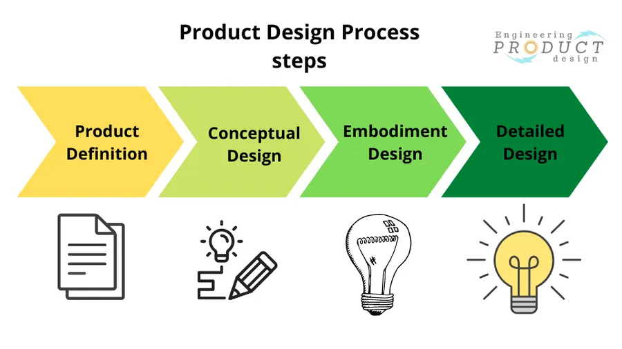
Choosing the Right PCB Design Ltd Partner: A Comprehensive Guide
In today's technologically driven world, PCB design is the backbone of countless electronic devices. PCB Design Ltd stands as a key player, providing crucial services that transform innovative ideas into tangible products. This article guides you through understanding the services offered by PCB Design Ltd and how to choose the right partner for your next project, ensuring a smooth journey from concept to final production.
Understanding the Core Services of PCB Design Ltd
PCB Design Ltd companies offer a suite of critical services that underpin the development of electronic devices. These services encompass the entire lifecycle of a printed circuit board, from initial conception to physical prototyping. Understanding these core services is crucial for any client looking to engage a PCB design partner.
- Schematic Capture
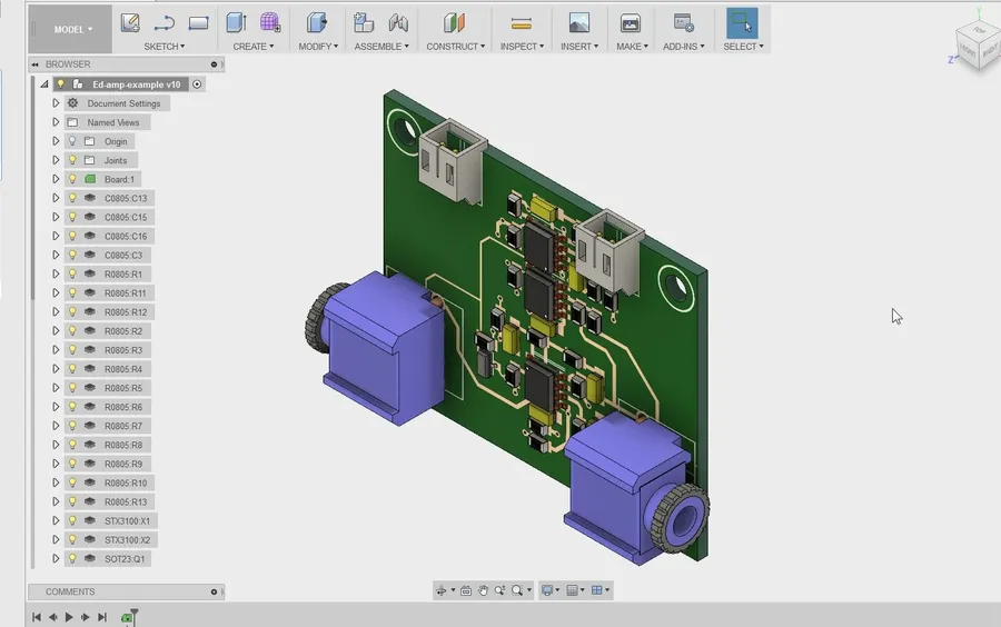
This initial phase involves translating a circuit's functional design into a detailed electronic diagram. It uses specialized software to represent components and their interconnections accurately. The schematic serves as the blueprint for the subsequent PCB layout and is a foundational step. - PCB Layout
Once the schematic is finalized, the PCB layout process involves physically arranging components and routing conductive traces on the board. This requires expertise in optimizing signal integrity, thermal management, and manufacturability. Proper layout is vital for the reliability and performance of the final product. - Simulation and Analysis
Before physical production, simulations are performed to assess the performance of the PCB design. This includes signal integrity analysis, thermal analysis, and electromagnetic compatibility (EMC) testing. Simulation helps identify and correct potential issues early in the design cycle, reducing costly rework. - Prototyping
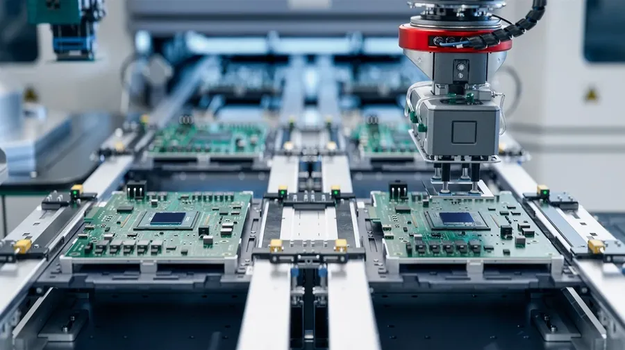
After design and simulation, physical prototypes are fabricated for testing. This phase verifies the design's functionality in a real-world environment. Prototypes allow for final design adjustments before large-scale production and are crucial in identifying unforeseen problems.
Key Considerations When Choosing a PCB Design Ltd Partner
Selecting the right PCB design partner is crucial for the success of any electronic product development. This decision requires careful evaluation of several key factors, ensuring the chosen partner aligns with your specific project requirements and business objectives. These factors include, but are not limited to experience, expertise, geographic location, and company size.
- Experience and Track Record
A company's history and past performance offer tangible evidence of their capabilities. Look for a partner with a proven track record of successful projects similar to yours, demonstrating they possess the necessary skills and experience. - Technical Expertise and Specialization
PCB design is not monolithic; it encompasses diverse technologies and applications. Ensure the partner has expertise in the specific areas relevant to your project, such as high-speed design, RF circuits, or specific industry standards. - Geographic Location and Communication
The location of your PCB design partner can influence project timelines, communication efficiency, and logistical considerations. While remote collaboration is common, consider time zone differences and the potential need for in-person meetings. - Company Size and Resources
The size of a PCB design company can impact its ability to handle your project's scope and complexity. Smaller firms may offer more personalized attention, while larger firms may have more resources and capacity for large-scale projects. Match their resources to your project's demands. - Software and Technology Proficiency
Confirm the partner's proficiency with the latest design tools and technologies, including the software they will use for schematic capture, layout, and simulation. Compatibility and the ability to work in your preferred workflow are critical. - Quality Assurance and Certification
A reputable PCB design partner should adhere to rigorous quality control standards and industry best practices. Look for certifications like ISO 9001 or similar, as this indicates a commitment to quality and reliability.
Prior to committing to a partnership, it's essential to ask direct questions to gauge a PCB Design Ltd company's suitability. These questions should probe into their specific capabilities and processes.
- Key Questions to ask Potential PCB Design Partners
What is your team's experience with projects similar to ours? Can you provide case studies or references showcasing your work? What PCB design software and technologies do you utilize? Do you have experience in designing for our specific industry? What is your quality control process? How do you ensure designs meet specifications? What is your approach to project management? How do you handle revisions and project change requests? What is your pricing structure, and are there any potential additional fees to be aware of? What is your policy regarding intellectual property? What is your turnaround time for this specific type of project?
The Importance of Full Product Design Services
Engaging a PCB design company that provides comprehensive, end-to-end product design services offers significant advantages, streamlining the development process from initial concept to final manufacturing. This integrated approach minimizes risks, enhances product quality, and fosters a more efficient project workflow.
- Reduced Project Risk
By working with a single entity for all stages of product development, potential communication gaps and errors arising from multiple vendors are minimized. This integrated approach ensures that design, manufacturing, and testing processes align seamlessly, reducing the likelihood of costly revisions or delays. - Enhanced Product Quality
A cohesive approach to product development, where the same team manages all aspects, allows for a better understanding of the design's nuances and its impact on manufacturing. This continuity ensures higher design integrity and reduces the risk of errors during transfer between different teams or companies, leading to a superior end product. - Streamlined Communication
Having a single point of contact simplifies project management, facilitating clearer and more efficient communication. This approach allows for quicker issue resolution and better overall control of the project's progress. A single team working in unison, rather than multiple independent teams, leads to more effective decision-making and implementation, saving both time and cost. - Faster Time-to-Market
By streamlining workflows and reducing the coordination burden between different entities, a comprehensive approach can significantly reduce the overall project timeline, allowing for faster product launches. An end-to-end service eliminates the need for coordinating handoffs between different teams, therefore accelerating the entire development process.
PCB Design Ltd: Capabilities in Various Industries
PCB Design Ltd's expertise is not confined to a single sector; their services span a multitude of industries, demonstrating a remarkable adaptability and a deep understanding of diverse design requirements. This broad applicability is a key strength, enabling them to address the unique challenges of various technological domains.
Below are some notable industries where PCB Design Ltd's services are frequently utilized:
- Aerospace and Aviation
In aerospace, where reliability is paramount, PCB Design Ltd provides designs for avionics, control systems, and communication devices. These designs often require high-density interconnects and must withstand harsh environmental conditions, adhering to stringent standards such as DO-254. - Medical Devices
The medical field demands precision and adherence to strict regulatory requirements. PCB Design Ltd supports the development of diagnostic equipment, patient monitoring systems, and implantable devices, often complying with standards like ISO 13485 and IEC 60601. Their work in medical device PCBs involves highly sensitive analog circuitry and low-power consumption designs. - Automotive
The automotive industry is experiencing a rapid increase in electronic content, from engine management systems to advanced driver-assistance systems (ADAS). PCB Design Ltd contributes by providing PCB designs that are robust, reliable, and capable of handling the extreme conditions present in automotive environments. These designs often incorporate high-speed data transmission and sophisticated power management. - Telecommunications
In the fast-paced telecommunications sector, PCB Design Ltd creates designs for network equipment, wireless devices, and satellite communication systems. Their expertise includes high-frequency design techniques, impedance matching, and signal integrity analysis to ensure optimal performance of communication circuits. - Industrial Automation
Industrial automation requires robust and reliable PCBs for control systems, sensors, and robotic applications. PCB Design Ltd offers designs tailored to the demands of industrial environments, which include durability to withstand electromagnetic interference, temperature variations, and mechanical stress. These designs emphasize dependable, long-term performance. - Consumer Electronics
For consumer electronics, where miniaturization, cost efficiency, and high production volumes are key, PCB Design Ltd creates compact and high-performance designs for devices like smartphones, wearables, and smart home devices. This requires expertise in RF design, HDI (High-Density Interconnect) technology, and cost-effective manufacturing processes. - Renewable Energy
The renewable energy sector, encompassing solar, wind, and battery storage solutions, relies on dependable electronic systems. PCB Design Ltd contributes by designing robust PCBs for energy conversion, management, and monitoring systems. These designs frequently include power electronics components and require high efficiency and reliability to handle variable energy loads.
This diverse application across various sectors highlights PCB Design Ltd's capability to adapt their expertise to the specific requirements of each industry. Their proven track record in delivering reliable and effective PCB designs across this spectrum makes them a versatile and trusted partner for product development.
Frequently Asked Questions About PCB Design and PCB Design Ltd
This section addresses common questions about PCB design, providing clear answers to help you better understand the field and the services offered by companies like PCB Design Ltd.
- What does PCB design stand for?
PCB design stands for Printed Circuit Board design. It is the process of creating the layout and structure of a board that connects electronic components, enabling them to function as intended in an electronic device. - How much does PCB design cost per hour?
The cost of PCB design per hour varies significantly depending on factors such as the complexity of the design, the experience level of the designer or company, and the geographic location. Hourly rates can range from $50 for junior designers to $200+ for senior designers or specialized firms. Project-based pricing is also common. - Is PCB design worth learning?
Yes, PCB design is a valuable skill to learn, especially for those in electronics, engineering, and related fields. The demand for PCB designers remains high, with opportunities spanning various industries. It's a fulfilling career path for those with a keen interest in electronics and spatial reasoning. - Which is the best PCB design software?
The 'best' PCB design software depends on specific needs and preferences. Popular options include Altium Designer, Eagle, KiCad, and OrCAD. Altium Designer is known for its comprehensive capabilities, while KiCad is a powerful open-source solution. Choosing depends on factors like budget, project complexity, and user experience. - What factors affect the cost of PCB design services?
Several factors influence the cost of PCB design services including, but not limited to, design complexity (number of layers, component density), project urgency, the need for specific design features (impedance control, high-speed design), expertise required, and the type of deliverables. A detailed analysis is typically needed to estimate project expenses accurately. - What are common challenges in PCB Design?
Common challenges in PCB design include managing signal integrity, preventing electromagnetic interference, optimizing thermal management, adhering to manufacturability guidelines, and achieving cost-effective designs. Addressing these requires in-depth understanding of materials, design tools, and fabrication processes. - What are the different types of PCB?
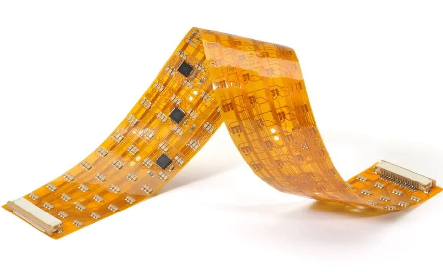
PCBs come in various types, the most common being single-layer, double-layer, and multi-layer. Others include flexible PCBs, rigid-flex PCBs, and metal-core PCBs. The choice depends on the application's requirements, cost considerations, and design constraints. Each type has specific performance characteristics that must be considered.
Comparing PCB Design Options: In-House vs. Outsourcing
Deciding whether to handle PCB design in-house or to outsource it to a specialized firm like PCB Design Ltd is a critical strategic decision with significant implications for project timelines, costs, and overall quality. This section provides a detailed comparison to help you make an informed choice.
| Factor | In-House PCB Design | Outsourcing to PCB Design Ltd |
|---|---|---|
| Expertise | Potentially limited to the skills of the existing team; may require training and development. | Access to a team of experienced and specialized PCB designers with diverse skill sets. |
| Cost | Initial investment in software, hardware, and training can be significant; ongoing operational costs, salaries, benefits, and possible retraining also need to be considered. | Variable project costs depending on design complexity; more predictable overall expenses. |
| Control | Direct control over the design process and timelines. | Shared control; requires close coordination and clear communication. |
| Speed and Efficiency | Potentially slower due to learning curves, resource constraints, and the lack of specialized tools. | Typically faster turnaround times due to specialized tools, streamlined processes, and experienced staff. |
| Scalability | Difficult to scale up or down quickly, resulting in bottlenecks or underutilized resources. | Easily scalable to handle fluctuating project demands. |
| Focus | May divert internal resources from core competencies and other strategic priorities. | Allows internal teams to focus on core business areas and product strategy. |
| Software and Tools | Requires investment in and maintenance of PCB design software and related tools. | Utilizes industry-standard tools and software, reducing your capital outlay. |
| Risk Management | Higher risk of errors and delays due to lack of specialized expertise. | Lower risk due to the expertise and experience of specialized PCB design teams. |
Ensuring Quality and Reliability in PCB Design with PCB Design Ltd
Achieving high-quality and reliable PCB designs requires a meticulous approach, with a focus on adherence to stringent processes and industry standards. A reputable PCB design company like PCB Design Ltd implements rigorous quality control measures at every stage of the design and manufacturing process, to minimize risk and ensure optimal performance.
- Design for Manufacturability (DFM)
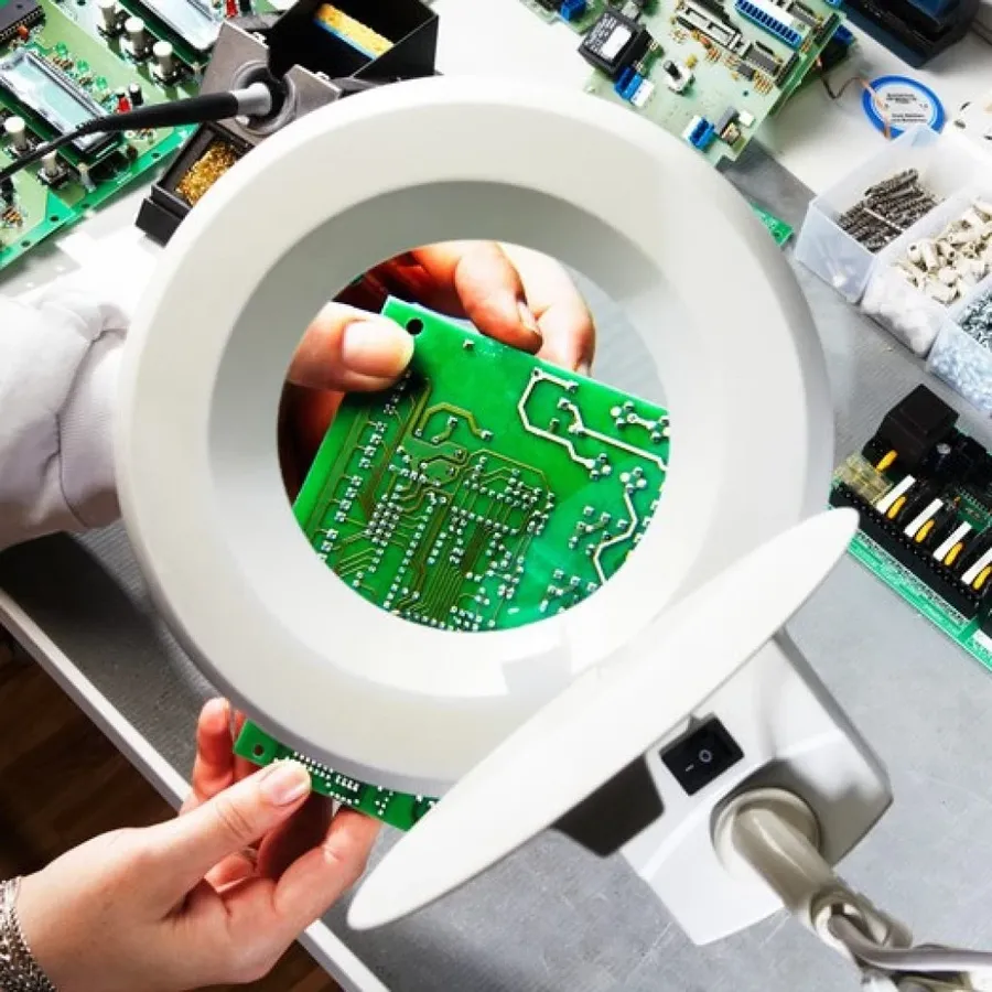
DFM analysis is essential to ensure that a PCB design can be efficiently and reliably manufactured. This involves reviewing the design for manufacturability issues, such as trace widths, spacing, and via placement, and making necessary modifications before fabrication. This step helps to reduce costs and improve yield rates. - Rigorous Design Reviews
A thorough design review process is critical. This involves multiple stages, including internal reviews by the design team, peer reviews by other engineers, and formal reviews with the client. These reviews are structured to catch errors early in the design process, minimizing costly corrections later. - Adherence to Industry Standards
Compliance with industry standards such as IPC standards for PCB design and manufacturing is paramount. These standards provide guidelines for material selection, design rules, and quality control procedures, ensuring that the final product meets the highest levels of reliability and performance. - Material Selection
Choosing the right materials is crucial for both performance and reliability. The selected materials must withstand the expected operating conditions (temperature, humidity, voltage, etc.), possess the required electrical properties, and meet environmental requirements (RoHS compliance). PCB Design Ltd ensures that only certified and reliable materials are used in their products. - Simulation and Testing
Before physical prototyping, PCB designs undergo rigorous simulations to analyze signal integrity, thermal performance, and mechanical stress. This virtual prototyping stage helps identify and correct potential issues early, ensuring better performance and reliability. Physical testing is also critical, verifying the design's performance and detecting manufacturing defects. - Documentation and Traceability
Complete documentation of the design and manufacturing process is essential. Detailed specifications, assembly instructions, and testing reports are generated and stored systematically. Full traceability of each PCB is ensured, which can prove invaluable in diagnosing issues and enhancing future revisions.
Future Trends in PCB Design and PCB Design Ltd's Role
The landscape of PCB design is continually evolving, driven by advancements in technology and the increasing complexity of electronic devices. Companies like PCB Design Ltd are not just participants in this evolution but also play a crucial role in shaping it. Understanding these trends is essential for businesses seeking to stay competitive and innovative.
Several key trends are poised to define the future of PCB design. These include:
- Miniaturization and High-Density Interconnect (HDI)
As devices shrink in size, the demand for smaller, more densely packed PCBs increases. HDI technology, with its finer lines and vias, allows for more functionality in less space. PCB Design Ltd must stay at the forefront of this technology to meet the demand for compact electronic solutions. - Flexible and Stretchable Electronics
The rise of wearables and flexible displays drives the need for PCBs that can bend and conform to non-planar surfaces. This involves new materials and manufacturing techniques that PCB Design Ltd needs to incorporate in its design processes. - Advanced Materials
Traditional PCB materials are being challenged by the need for higher operating frequencies and improved thermal management. Materials with lower dielectric constants and better thermal conductivity will be increasingly important, requiring PCB Design Ltd to develop design rules and techniques for these materials. - Artificial Intelligence (AI) and Machine Learning (ML) in Design Automation
AI and ML are being used to automate many aspects of PCB design, including routing, placement, and design rule checking. This will allow PCB Design Ltd to expedite development cycles and optimize board performance. As AI matures, PCB design will become more efficient and less error-prone. - Integration of 3D Printing for Prototyping
3D printing is rapidly becoming a viable option for rapid PCB prototyping, which can significantly reduce the time and cost of bringing new designs to market. PCB Design Ltd's strategy should include incorporating 3D printing technology into its prototyping workflow to reduce turnaround time and enable quicker design revisions. - Sustainability and Eco-Friendly Design
Growing environmental concerns are pushing for more sustainable PCB designs and manufacturing processes. PCB Design Ltd is expected to adopt lead-free soldering, reduce material waste, and explore the use of recyclable materials.
PCB Design Ltd's role in these trends is multifaceted. They must not only adapt to these advancements but also actively drive innovation by investing in R&D, incorporating new design tools, and training their engineers on the latest technologies. The company's ability to anticipate and integrate these future trends will be vital to their continued success and leadership in the PCB design industry.
Selecting the right partner for your PCB design needs is crucial for successful product development. PCB Design Ltd plays a significant role in this process, offering comprehensive solutions from concept to manufacturing. By understanding the key considerations, services, and future trends outlined in this article, you can make informed decisions to ensure the success of your projects with PCB design companies like PCB Design Ltd. As technology advances, having a strategic design partner like PCB Design Ltd will be increasingly important to turn innovative ideas into reality.