Effortless PCB Design Online: A Comprehensive Guide
In today's fast-paced world, the ability to design circuit boards online has revolutionized electronics development. Gone are the days of complex software installations and limited access. Online PCB design platforms now empower engineers, hobbyists, and students to bring their innovative ideas to life from anywhere with an internet connection. This article dives into the best online tools available, offering a roadmap to seamless circuit board creation and highlighting the key considerations for successful projects.
Introduction to Online PCB Design Platforms
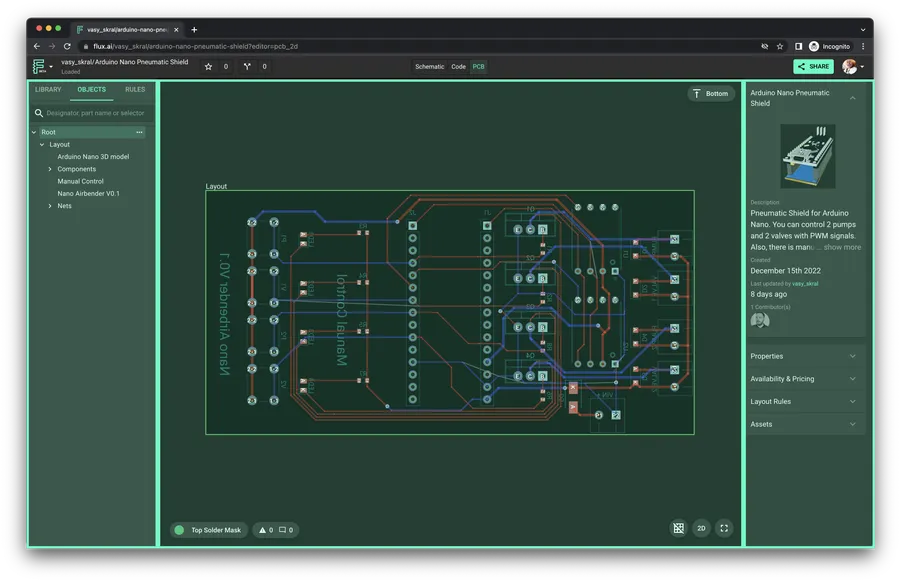
Online PCB design platforms represent a paradigm shift from traditional desktop-based software, offering a cloud-based approach to designing printed circuit boards. These platforms provide engineers and hobbyists with unprecedented accessibility, collaboration capabilities, and often reduced upfront costs, making them an increasingly essential tool in today's fast-paced electronics development landscape.
Traditional PCB design software typically involves high licensing fees, powerful desktop workstations, and complex installation processes. In contrast, online PCB design platforms operate directly within a web browser, eliminating the need for software installations, updates, or dedicated hardware. This fundamental difference provides significant advantages in terms of accessibility, flexibility, and cost-effectiveness.
Key Features to Look for in PCB Design Online Tools
Selecting the right online PCB design tool is crucial for an efficient and successful design process. The ideal platform will offer a suite of integrated features that cater to both novice and experienced users, streamlining the journey from concept to fabrication. This section details the essential functionalities that should be considered when evaluating online PCB design software.
User-friendliness is paramount. A clear, intuitive interface reduces the learning curve and allows for efficient navigation and design. Tools should also provide robust functionality, including schematic capture for creating circuit diagrams, a versatile PCB layout tool to place and connect components, and comprehensive component libraries with regularly updated part data. Integrated simulation tools are essential for verifying the design's functionality, and collaboration features are crucial for team projects.
| Feature | Description | Importance |
|---|---|---|
| Schematic Capture | Tool for creating circuit diagrams, representing electrical connections between components. | Fundamental for defining the circuit's functionality; a good schematic reduces errors. |
| PCB Layout Tools | Software for arranging components and routing connections on the PCB. | Critical for the physical implementation of the design, affecting signal integrity and manufacturability. |
| Component Libraries | Database of electronic components with associated symbols, footprints, and parameters. | Essential for quick and accurate part selection; reduces manual errors and ensures compatibility. |
| Simulation Capabilities | Features to simulate circuit behavior, verifying performance before fabrication. | Important for identifying and correcting design flaws early in the development phase. |
| Real-time Collaboration Options | Tools that enable multiple designers to work on the same project simultaneously. | Crucial for team projects, improving efficiency and reducing design time. |
| Integration with Manufacturers | Capabilities to generate manufacturing files (Gerber) and connect directly to PCB manufacturers. | Simplifies the transition from design to production, making the process more efficient. |
Top Free Online PCB Design Software: A Detailed Comparison
Selecting the right PCB design software is crucial for efficient and accurate board development. This section provides a comparative analysis of popular free online PCB design tools, highlighting their capabilities, strengths, limitations, and target user profiles to assist designers in making informed decisions.
| Software | Schematic Capture | PCB Layout | Component Libraries | Simulation | Collaboration | Strengths | Limitations | Ideal User |
|---|---|---|---|---|---|---|---|---|
| EasyEDA | Yes | Yes | Extensive, Cloud-Based | Basic | Yes, Real-time | User-friendly, large component library, seamless integration with JLCPCB for manufacturing | Limited advanced simulation capabilities | Beginners and hobbyists looking for ease of use and quick prototyping |
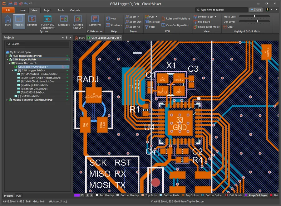
| CircuitMaker | Yes | Yes | Extensive, Cloud-Based | Basic | Yes | Powerful layout tools, extensive cloud libraries | Steeper learning curve compared to EasyEDA, requires Altium account | Experienced users and professionals who prioritize power and functionality |
| LibrePCB | Yes | Yes | Growing, Local | No | No | Open-source, cross-platform, no vendor lock-in | Still under development, smaller community, not cloud-based. | Users who prioritize open-source solutions and have a preference for desktop applications |
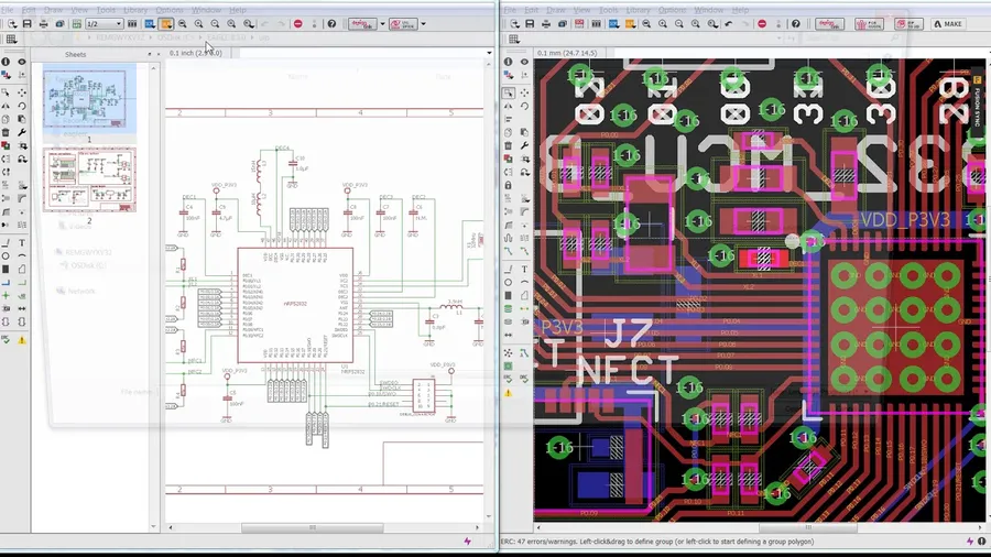
| KiCad | Yes | Yes | Extensive, Local | Limited | No, requires external tools for collaborative editing | Powerful, open-source with active community and advanced features. No project size limit. | Steep learning curve, requires local setup | Professional engineers and advanced users needing no limits on project size and prefer complete control over their design workflow |
Advanced Features in Online PCB Design Tools
Online PCB design tools have evolved to incorporate sophisticated functionalities that streamline complex projects and elevate design quality. These advanced features, once exclusive to desktop software, are now accessible through cloud-based platforms, offering professionals and advanced hobbyists powerful capabilities for designing high-performance PCBs.
| Feature | Description | Benefits |
|---|---|---|
| Signal Integrity Analysis | Simulates signal behavior to identify and resolve potential issues like reflections and crosstalk. | Ensures signal quality, minimizes signal degradation, and improves overall system reliability. |
| 3D Visualization of PCBs | Displays a three-dimensional rendering of the PCB design, allowing for a detailed view of the component placement and board structure. | Enhances design understanding, facilitates the identification of mechanical interference, and improves communication among team members. |
| Autorouting Capabilities | Automatically routes traces on the PCB, reducing design time and enabling complex designs to be completed more efficiently. | Significantly accelerates the design process, minimizes manual routing errors, and is essential for designing PCBs with a large number of components and complex layouts. |
| Differential Pair Routing | Provides tools to route differential pairs of traces with precise matching. | Improves signal integrity for high-speed signals by minimizing noise and signal distortion |
| Impedance Control | Allows for the precise control of trace impedance by adjusting trace width and distance between trace and ground plane. | Ensures signals transmit with minimal reflection for optimal performance of high speed digital and analog systems. |
These features are crucial in professional settings, where performance and reliability are critical. By incorporating signal integrity analysis, designers can preempt issues that could compromise functionality; 3D visualization aids in ensuring fit and assembly, and autorouting significantly reduces the time spent on layout. The integration of these advanced capabilities directly addresses the needs of professionals aiming to design high-quality and reliable PCBs.
From Schematic to Layout: A Step-by-Step Online PCB Design Process
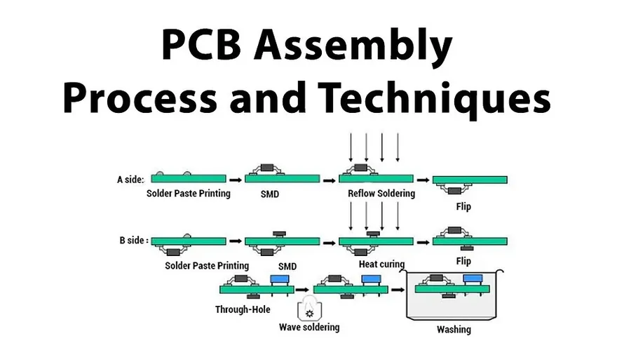
Online PCB design tools streamline the creation of printed circuit boards, guiding users from initial schematic capture to final Gerber file generation. This process typically encompasses several key stages, each crucial for a successful design outcome, utilizing the collaborative and accessible nature of cloud-based platforms.
- Schematic Capture
Begin by creating a schematic diagram using the online tool's editor. This involves placing and connecting electronic components, which may be selected from integrated libraries or custom-created, to represent the circuit's logical connections. - Component Selection
Choose components from the tool's libraries or import custom components. Verify the selected components match the specifications and requirements of your design, ensuring that they are available and correctly modeled for both simulation and manufacturing. - Board Layout
Define the physical dimensions of the PCB and place components onto the board in a manner that minimizes signal path lengths, reduces interference, and accommodates physical constraints. Consider component placement in relation to heat dissipation and manufacturing. - Routing
Connect components on the layout using the tool's routing capabilities, defining the paths for electrical signals on the PCB. The aim is to minimize signal impedance and interference by optimizing trace widths and utilizing appropriate layer strategies. Use autorouting tools judiciously, opting for manual routing for critical paths. - Design Rule Check (DRC)
Run a Design Rule Check to ensure compliance with manufacturing guidelines and electrical constraints. Address all warnings and errors to prevent production issues and ensure the board meets the required specifications. - Gerber File Generation
Generate Gerber files from the final PCB design. These files are the industry standard for PCB manufacturing, containing all necessary information to produce the physical board. Inspect Gerber files to ensure data integrity before submitting them for manufacturing.
Specific tips to avoid common design errors include: performing regular design backups, implementing proper ground planes, and double-checking the datasheets of all components.
Utilizing Online Component Libraries and Resources
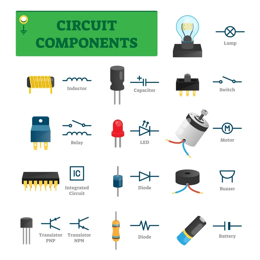
Efficiently leveraging online component libraries and resources is crucial for streamlined and accurate PCB design. These libraries provide pre-built models and datasheets, which significantly reduce design time and the likelihood of errors, enabling designers to focus on innovation rather than tedious component creation.
Here's a breakdown of how to effectively use these resources:
- Accessing Component Libraries
Most online PCB design tools provide access to vast component libraries. These libraries typically include both schematic symbols and PCB footprints for various components. Use the search functionality within these libraries to find specific parts by name, manufacturer, or part number. - Utilizing Datasheets
Always cross-reference component selections with their datasheets. Datasheets provide critical information such as pinouts, electrical characteristics, and recommended operating conditions. This step is essential for avoiding design errors and ensuring proper functionality. - Managing Components Effectively
Organize components within your design for better clarity and management. Many platforms allow users to create custom libraries or folders for project-specific components. This ensures you are using the correct parts throughout the design process. - Leveraging Cloud-Based Resources
Cloud-based component libraries allow multiple designers to access and share the same parts, ensuring uniformity and version control in collaborative projects. This also reduces the need for maintaining local component libraries and facilitates better design consistency. - Custom Component Creation
If a needed component is not found in existing libraries, most online tools provide functionality to create custom parts. This often involves drawing a schematic symbol, defining the footprint, and then linking it to the necessary datasheets. Ensure accuracy in custom component creation, as inaccuracies can lead to board issues.
By following these practices, users can optimize their design process, improve component accuracy, and ensure manufacturability.
Collaboration and Sharing in Online PCB Design
Online PCB design platforms have revolutionized collaborative engineering, allowing multiple designers to contribute to the same project concurrently, thereby accelerating the development cycle and enhancing team productivity. These platforms facilitate real-time interactions, version control, and seamless sharing of design data, effectively transforming the way PCB design teams operate.
- Real-Time Collaboration
Multiple team members can access and modify a PCB design simultaneously, seeing changes reflected instantly. This eliminates the traditional bottlenecks associated with sequential design processes and allows for parallel problem solving. - Version Control
Online platforms maintain a comprehensive history of design changes, enabling easy tracking, rollback to previous versions, and the avoidance of conflicts from simultaneous edits. This is a crucial feature for ensuring design integrity. - Shared Component Libraries
Teams can create and access shared libraries of components, ensuring consistency across projects. This promotes reuse of established components and prevents the use of obsolete or incorrect parts in designs. - Annotation and Feedback
Designers can add annotations, notes, and comments directly onto the PCB layout, facilitating clear communication and providing context for design decisions. This feature is invaluable for complex designs and large teams. - Permission Control
Project managers can set access permissions to control who can view, edit, and share designs. This ensures that sensitive data is protected while still facilitating collaboration within the team. - Integration with Other Tools
Online PCB platforms often integrate with other team communication and project management tools, further streamlining collaboration workflows.
Frequently Asked Questions about Online PCB Design Tools
This section addresses common concerns and questions that arise when considering online PCB design tools. We aim to provide clear, concise answers to help new and experienced users understand the nuances of this approach to PCB design, covering topics from accessibility and security to data management and cost.
- Are online PCB design tools as capable as traditional desktop software?
Online PCB design tools have evolved significantly and now offer comparable functionality to desktop software for many design tasks. While some extremely specialized features might still be exclusive to desktop platforms, cloud-based solutions provide a robust set of tools suitable for a majority of PCB design projects. They often boast advantages in accessibility, real-time collaboration, and automatic updates. - Is my design data secure when using online PCB design platforms?
Reputable online PCB design platforms implement robust security measures, such as data encryption, secure servers, and regular security audits, to protect user data. It is essential to choose platforms that adhere to industry security standards and have a clear privacy policy. Always utilize strong, unique passwords and be aware of any data sharing settings on the platform. - What happens to my design files if my subscription expires or I lose internet connectivity?
Most online PCB design platforms store your design files in the cloud, allowing you to access them as long as your subscription is active. In the event of subscription expiration, many platforms offer options to export your design files in common formats like Gerber or EAGLE for local storage. If your internet connection is interrupted, most systems store a local version, allowing you to continue to work, but synchronization may not occur until your internet is restored. It is recommended to periodically back up your files locally in case of unexpected outages or changes in provider services. - Do online PCB design tools offer component libraries and how frequently are they updated?
Yes, online PCB design platforms typically provide extensive component libraries that are continually updated to include new components. These libraries are crucial for accurate design and component management. Users can often import custom parts if not found in the library. Ensure that the platform you choose offers a library of the parts you need and updates it regularly. - What are the main advantages of online PCB design over offline methods?
Online PCB design offers several advantages, including accessibility from any device with an internet connection, real-time collaboration, automatic updates, and often lower initial costs compared to expensive desktop software licenses. Additionally, many online platforms have built-in version control that simplifies design management. Cloud-based platforms also remove the burden of managing complex software installations or updates. - Are there free options available for online PCB design?
Many online PCB design platforms offer free versions or free trials that provide a fully functional set of tools sufficient for learning and many small to mid-sized projects. These free tiers may have limitations, such as reduced storage, fewer features, or restrictions on project collaboration, but are generally a great starting point before committing to a paid plan. - How do online PCB design tools handle simulation and signal integrity analysis?
Many of the more advanced online PCB design platforms are integrating features for simulation and signal integrity analysis to ensure that designs are sound. These tools are crucial for identifying and correcting signal integrity issues, such as impedance mismatches, noise, and crosstalk, before fabrication.
Tips for Optimizing Your Online PCB Designs
Optimizing PCB designs within online platforms is crucial for achieving desired performance, manufacturability, and cost-effectiveness. The convenience of online PCB design tools makes it easier to iterate and refine designs, but specific strategies must be employed to fully leverage their capabilities and produce high-quality results. This section provides practical advice for optimizing layout, routing, and overall design for manufacturability within the online environment.
- Prioritize Component Placement
Strategic component placement is the foundation of a well-optimized PCB. Group related components together to minimize trace lengths, reduce signal interference, and simplify routing. Place heat-generating components in areas with good thermal dissipation. Consider the physical constraints of your enclosure and the accessibility of test points during layout. - Optimize Layer Stack-Up
Carefully choose your layer stack-up for optimal impedance control and signal integrity, especially when working with high-speed circuits. Consider the number of signal layers, ground layers, and power layers to minimize noise and cross-talk. Work with your manufacturer to ensure the stack-up is suitable for your manufacturing process. - Efficient Routing Techniques
Employ efficient routing techniques such as keeping traces as short and direct as possible. Avoid sharp bends in traces to reduce impedance mismatches. Use differential routing where applicable, especially for high-speed signals to maintain signal quality and minimize EMI. Maintain consistent trace width to preserve impedance characteristics along the trace. - Utilize Ground Planes and Vias Effectively
Use large ground planes to provide a low impedance return path and reduce noise. Use vias effectively to ensure a good connection between layers. Avoid using vias on sensitive signal paths when possible. Always design for manufacturability with via size and spacing in mind. - Design for Manufacturability (DFM)
Consider Design for Manufacturability (DFM) guidelines to reduce manufacturing costs and errors. Ensure sufficient spacing between components and traces for the capabilities of your manufacturer. Consider component footprint accuracy and pad sizes. Use standard component packages whenever possible. The online design tools can often check for basic DFM issues, but manual review is crucial. - Leverage Online Simulation Tools
Utilize any available online simulation capabilities, such as signal integrity analysis, to identify potential problems before physical prototyping. Run thermal simulations if necessary, to pinpoint potential hotspots. Verify power distribution networks to ensure components receive adequate current and voltage. - Regularly Review and Verify Your Design
Regularly review your design during the entire process. Check your schematic against your layout, verify the component connections, confirm the layer stack-up, and perform a final design rule check (DRC) before generating the manufacturing files. Remember the online platform is a tool, and a methodical design process is still essential. Get multiple set of eyes to review the design to catch potential mistakes.
The rise of online PCB design has significantly lowered the barrier to entry for creating custom circuit boards. By leveraging accessible and powerful tools, anyone can now take advantage of PCB design online for prototyping and production. Whether you're a student, hobbyist, or seasoned engineer, the convenience, collaboration, and advanced features of online platforms make it an ideal environment for bringing electronic projects to life, all while streamlining the design to manufacturing pipeline.