Effortless PCB Design with EasyEDA Online: A Comprehensive Guide
In today's fast-paced tech world, designing electronic circuits and PCBs often feels like a daunting task. But what if I told you there's a powerful, free tool that makes it accessible to anyone? Enter EasyEDA online, a browser-based platform that simplifies the entire process, from schematic capture to PCB layout. Whether you're a seasoned engineer or a hobbyist taking your first steps, EasyEDA's intuitive interface and robust features have revolutionized PCB design, making it as accessible as using a web browser. This article will guide you through the ins and outs of EasyEDA online, highlighting its capabilities and how it can empower you to bring your electronic projects to life with ease.
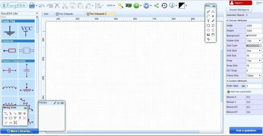
Getting Started with EasyEDA Online
EasyEDA Online provides a streamlined and accessible platform for electronic design, removing the complexities of traditional desktop software. This section will guide you through the initial steps, from creating your free account to understanding the core interface elements. The goal is to have you quickly navigating the dashboard, managing your projects, and feeling comfortable with the basic tools available.
- Account Creation
Visit the EasyEDA website and create a free account using your email address or a third-party login. The free version offers all the core functionality for personal and educational use. - Dashboard Overview
The dashboard is your central hub, displaying all active projects, recent activity, and team invitations. The interface is designed to be user-friendly, allowing for easy access to your different designs and collaborative features. - Project Creation
To begin a new design, click 'New Project'. You will be prompted to give your project a name and select a basic structure. Consider using clear names to easily manage your projects. - Navigating the Interface
The interface consists of the main menu bar, a tool panel, the design canvas, and the project browser. Understanding these components is crucial to quickly work with the platform. The menu provides options for file management, editing, and setting preferences. The tool panel houses components, drawing, and simulation tools. The design canvas is where designs are created. The project browser allows the designer to switch between project files. - Basic UI Elements
Familiarize yourself with basic elements like zooming, panning, grid settings, and undo/redo functions, they are in the top menu bar or left side of the canvas. They are critical to efficient design. All the UI elements are intuitive and have descriptive labels.
Schematic Capture with EasyEDA
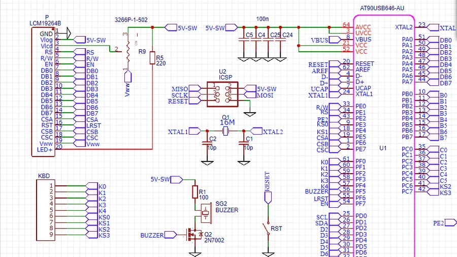
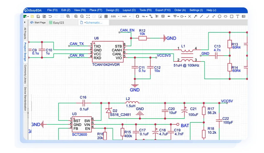
EasyEDA's online schematic editor provides a robust and intuitive environment for creating circuit diagrams, allowing users to seamlessly place components, connect wires, and design custom parts when required. This functionality is crucial for translating abstract electrical concepts into tangible designs ready for simulation and PCB layout.
The schematic capture process within EasyEDA involves several key steps. First, the user will access the schematic editor via their project dashboard. Second, components are placed from the extensive built-in library which is regularly updated. Third, wires are drawn to establish connections between components. Finally, annotations, notes, and net labels are added to complete and clarify the schematic diagram.
- Component Placement
EasyEDA provides a comprehensive component library that can be searched by keyword or filter to locate specific parts required for a circuit. Components can be placed, rotated, and mirrored directly on the schematic canvas with ease, ensuring the circuit diagram is arranged logically. - Wiring Connections
Connecting components is as simple as selecting the wire tool and connecting terminals of various components. Automatic net naming is present to improve readability, but custom names can be used if required. Various wire styles are available to denote different types of connections, improving the diagram's accuracy and clarity. - Custom Component Creation
If a necessary component is not available in the library, users have the option to create custom components using the built-in editor. This feature allows for the precise drawing of symbols, defining of pins, and adding associated component parameters for use in their projects. Furthermore, these custom components can be saved for future use, and shared within the community.
| Feature | Description |
|---|---|
| Extensive Component Library | Includes a vast selection of commonly used electronic components, from basic resistors to complex integrated circuits. |
| Custom Component Editor | Allows the creation of custom symbols and footprints, useful when standard library components do not suffice. |
| Real-Time Error Detection | Offers immediate visual feedback when connections are made in the circuit, preventing many basic connection errors before simulation. |
| Annotation and Net Labels | Allows detailed notes to be added to the schematic as well as net labels which improve the clarity and documentation of the design. |
Circuit Simulation in EasyEDA
EasyEDA's integrated circuit simulator offers a crucial step in the PCB design process, allowing engineers to rigorously test their circuit designs before committing to a physical layout. This capability enables the identification and rectification of design flaws early on, saving both time and resources by preventing costly errors that might otherwise emerge in the physical prototyping phase. The simulator facilitates a comprehensive analysis through various simulation types.
The simulation process in EasyEDA involves several key stages, each contributing to a thorough assessment of circuit performance. Initially, the circuit schematic, created using EasyEDA's schematic editor, is transferred to the simulator environment. The user then defines the specific parameters relevant to the desired simulation, such as the simulation type (DC, AC, or transient), component values, and the time-step. Following parameter specification, the simulator is initiated, calculating and displaying circuit responses. Results are visualized through various plots and graphs, enabling a detailed performance analysis. These steps are critical for validating the circuit behavior against design expectations.
| Simulation Type | Description | Typical Use Case |
|---|---|---|
| DC Analysis | Analyzes the circuit's behavior at a steady-state condition, with constant voltage or current sources. | Determining bias points and operating regions of transistors and other active components. |
| AC Analysis | Examines the circuit's response to sinusoidal signals over a range of frequencies. | Evaluating frequency response, filter characteristics, and impedance matching. |
| Transient Analysis | Evaluates the circuit's time-domain behavior in response to time-varying signals or switching events. | Analyzing the dynamic behavior of a system, including switching regulators and pulse circuits. |
Beyond basic simulations, EasyEDA's simulator includes features for advanced analysis, such as noise simulation and parameter sweeps. Noise simulation is particularly important for sensitive circuits, revealing potential interference and noise issues. Parameter sweeps, conversely, enable engineers to simulate how circuit performance changes with variations in component values, facilitating sensitivity analysis and fine-tuning of circuit parameters for optimal performance. These simulation capabilities collectively enhance circuit designs by revealing potential operational limitations before hardware fabrication.
PCB Layout Fundamentals with EasyEDA
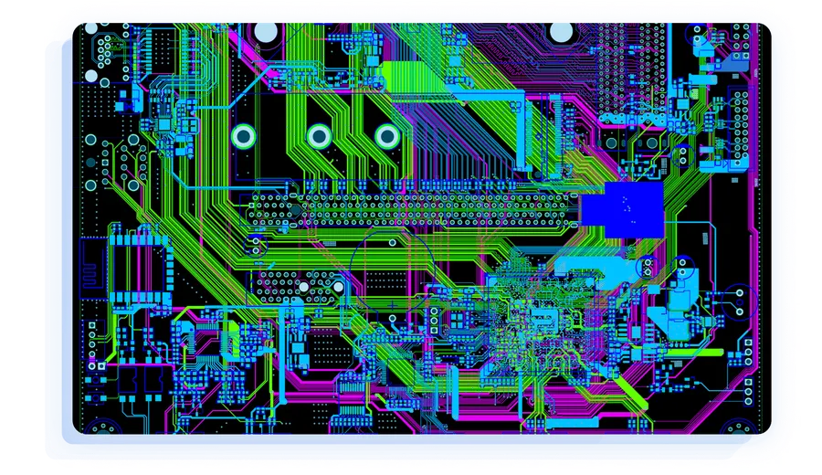
Transitioning from a schematic diagram to a physical printed circuit board (PCB) layout is a critical step in the electronics design process. EasyEDA streamlines this process by providing an intuitive online environment for component placement, trace routing, and multilayer board design. This section delves into the core aspects of PCB layout using EasyEDA, focusing on design rules, layer management, and best practices for achieving optimal board performance.
- Component Placement
Effective PCB layout begins with strategic component placement. Consider factors like signal flow, thermal management, and manufacturability when arranging components on the board. Group related components together to minimize trace lengths and improve signal integrity. - Trace Routing
Routing involves connecting component pins using conductive traces. EasyEDA offers various routing tools, including manual and auto-routing options. Aim for short, direct traces to reduce signal degradation and impedance mismatches. Adhering to impedance requirements is essential for high-speed signals. Furthermore, utilize wider traces for power signals to minimize voltage drop and current density. - Multilayer Board Design
EasyEDA supports multilayer board designs, which are crucial for complex circuits. Multilayer boards allow for increased routing density, dedicated power planes, and improved electromagnetic compatibility. Common multilayer configurations include 2-layer, 4-layer, and 6-layer boards. - Design Rules
Adhering to design rules is crucial for manufacturing success and optimal PCB performance. EasyEDA allows you to configure design rule checks (DRC) to prevent errors like trace spacing violations, pad overlap, and clearance issues. These design rules are typically dictated by the manufacturing process and specific requirements of the components used in your design. Always review the design rules provided by your manufacturer. - Layer Management
Understanding layer functions and proper layer assignments is essential. In a multi-layer PCB, layers can be utilized for signal routing, power and ground planes, as well as silkscreen and solder mask. Proper layering can minimize interference and maximize PCB performance.
| Aspect | Description | Best Practice |
|---|---|---|
| Component Placement | Arranging components on the PCB. | Group related components, consider thermal management, place decoupling capacitors close to IC pins. |
| Trace Routing | Connecting component pins with conductive paths. | Use short, direct traces, maintain consistent impedance, avoid sharp bends. |
| Via Placement | Connecting traces between different layers | Use vias judiciously, place them under components, maintain proper spacing from other traces. |
| Multilayer Boards | PCBs with multiple conductive layers. | Use inner layers for power and ground planes, optimize layer stack-up for signal integrity. |
| Design Rules | Specifications to ensure manufacturability and performance. | Adhere to minimum trace widths, clearances, and pad sizes as dictated by the manufacturer. Run DRC checks. |
Advanced PCB Design Features in EasyEDA
EasyEDA offers a suite of advanced PCB design features that extend beyond basic layout, enabling engineers to tackle complex designs with efficiency and precision. These tools include automated routing, comprehensive design rule checks (DRC), sophisticated file management capabilities, and advanced techniques for optimizing PCB performance.
- Auto-Routing
EasyEDA's auto-router simplifies the complex task of trace routing by automatically connecting components based on the schematic. While not a replacement for manual routing in critical areas, it significantly reduces routing time for non-critical nets. - Design Rule Checks (DRC)
The DRC feature ensures adherence to predefined design rules, preventing common errors such as overlapping traces, insufficient clearances, or incorrect via placements. This functionality greatly contributes to the reliability and manufacturability of the final PCB. - Importing and Exporting Files
EasyEDA facilitates seamless collaboration by supporting the import and export of various file formats, including Gerber files, which are essential for manufacturing, as well as other common formats used in electronic design such as DXF for importing mechanical outlines and SVG for graphical elements. - Polygon Pours
Polygon pours allow for the efficient creation of large copper areas, useful for ground planes and power planes. This improves signal integrity, thermal dissipation, and reduces impedance. - Via Stitching
Via stitching involves strategically placing vias to connect different layers of a PCB. This improves signal integrity, reduces impedance, and enhances the overall performance of multilayer PCBs. - Complex Routing Techniques
EasyEDA supports more complex routing techniques, such as differential pair routing, which are crucial for high-speed signal transmission. These tools provide users with precision in managing impedance and signal matching, essential for high-performance circuits.
| Feature | Description | Benefit |
|---|---|---|
| Auto-Routing | Automatically routes connections between components. | Reduces manual routing time, especially for less critical nets. |
| Design Rule Check (DRC) | Checks for rule violations such as trace overlap, clearance issues. | Ensures manufacturability and prevents errors before production. |
| File Import/Export | Supports various file formats (Gerber, DXF, etc.). | Enables collaboration and simplifies manufacturing preparation. |
| Polygon Pours | Creates large copper areas for ground/power planes. | Improves signal integrity and thermal dissipation. |
| Via Stitching | Connects different PCB layers with vias. | Enhances signal integrity and reduces impedance on multi-layer boards. |
| Differential Pair Routing | Routes differential signal pairs with controlled impedance. | Critical for high-speed signal transmission. |
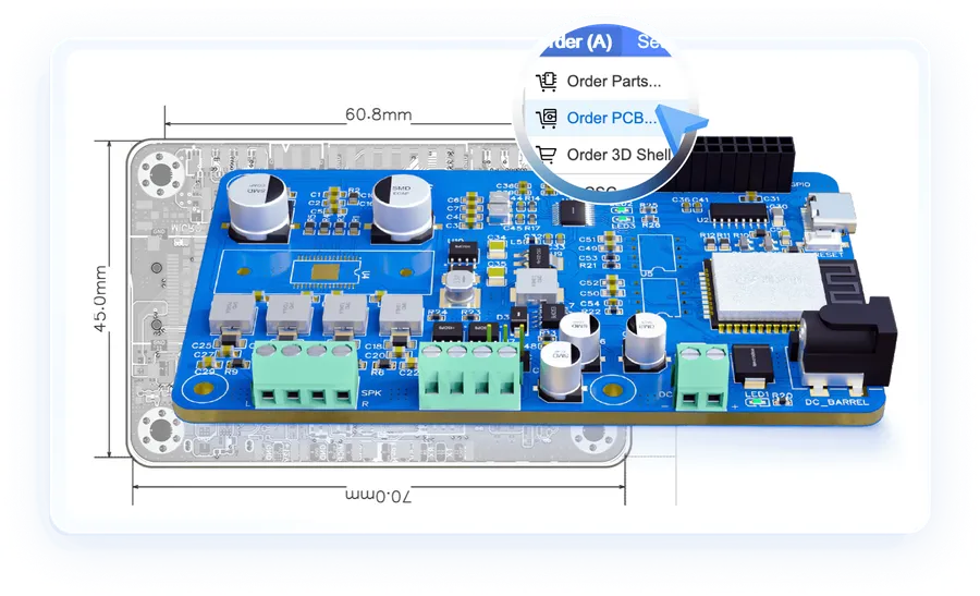
Integrating with JLCPCB for Manufacturing
Seamless integration with JLCPCB is a key advantage of using EasyEDA for PCB design, streamlining the transition from design to physical board. This section details the process of preparing your EasyEDA designs for manufacturing with JLCPCB, covering Gerber file generation, component sourcing, and direct ordering from the platform.
This integration simplifies the complexities of PCB manufacturing by allowing users to generate the necessary files (Gerber, drill, etc.), source components from JLCPCB's inventory, and place orders without leaving the EasyEDA environment. This approach not only speeds up the prototyping process but also ensures design compatibility with manufacturing requirements.
- Gerber File Generation
Learn how to accurately generate Gerber files from your EasyEDA PCB layout. This includes selecting the correct layers and settings to ensure that your manufacturing files meet JLCPCB's requirements. The process is largely automated, reducing the likelihood of human error. - Component Sourcing
Understand how to link components in your EasyEDA design to JLCPCB's parts catalog. This ensures you're using components readily available at JLCPCB, streamlining the assembly process. - Direct Ordering
Explore how to directly order your PCBs from JLCPCB using the integration within EasyEDA. This includes selecting board specifications, quantity, and shipping options. This integration simplifies what used to be a disjointed process, making the transition to manufacturing seamless.
Frequently Asked Questions About EasyEDA Online
This section addresses common inquiries regarding EasyEDA online, providing clear and concise answers to enhance user understanding and experience. We delve into the core functionalities and usage of this platform, resolving potential uncertainties.
- Is EasyEDA free to use?
Yes, EasyEDA offers a free version that provides a comprehensive suite of tools for schematic capture, PCB layout, and circuit simulation. This free version is suitable for hobbyists, students, and small-scale projects. However, EasyEDA also provides paid plans with more advanced features, such as a larger component library, more simulation resources and more cloud storage, catering to professional users with more complex design requirements. - Can I use EasyEDA offline?
No, EasyEDA is primarily an online platform, and thus it requires an active internet connection to access its functionalities. While it does not offer a fully functional offline mode, users can save their projects and libraries to their accounts, allowing them to resume their work on any device with internet access. This is one of the major distinctions between EasyEDA and its desktop-based competitors like KiCad, which can be used offline. - What are the main differences between EasyEDA and EasyEDA Pro?
EasyEDA Pro offers enhanced capabilities and resources compared to the free version. Key differences include: larger and more advanced component library, access to better support, more simulation capabilities with more powerful computational resources, an increased amount of cloud storage, and advanced design features like team collaboration. EasyEDA Pro is designed for professional users and those with more intricate design needs, while the free version is adequate for basic to medium complexity projects. - Which is the best free PCB design software?
The 'best' PCB design software depends heavily on the user's specific needs and preferences. However, both EasyEDA and KiCad are very popular and highly regarded as excellent options for free PCB design software. EasyEDA stands out for its cloud-based nature, intuitive interface, and seamless integration with JLCPCB for manufacturing. KiCad, on the other hand, is an open-source, desktop-based application that provides extensive customization and a very large and active community support network. The choice between the two depends on the user's preference for cloud vs desktop tools, and design complexity needs. - What file formats does EasyEDA support?
EasyEDA supports a variety of file formats for importing and exporting designs. For schematics, it supports its own native formats along with common formats such as .json, .svg, and .pdf. For PCB layouts, it supports Gerber files, which are the industry standard for PCB manufacturing, as well as .DXF for mechanical layouts. In addition, it can also import footprints and symbols from other EDA tools. - How does EasyEDA handle library management?
EasyEDA features a robust library management system, allowing users to access a vast online library of components. Users can also create custom symbols and footprints, organize them into personal libraries, and reuse them across multiple projects. This greatly accelerates the design process by avoiding the need to start from scratch each time.
Tips and Tricks for Efficient EasyEDA Design
Mastering EasyEDA involves not only understanding its features but also optimizing your workflow for maximum efficiency. This section provides practical tips and tricks to accelerate your design process, enhance your productivity, and streamline your overall experience within the EasyEDA online environment. Effective use of these techniques can significantly reduce design time and improve the quality of your final PCB.
- Keyboard Shortcuts
Leverage keyboard shortcuts to expedite common actions. For instance, use 'W' for wire, 'V' for via, 'C' for component selection. Familiarizing yourself with these shortcuts can substantially cut down design time. Refer to EasyEDA's official documentation for a comprehensive list. - Efficient Component Search
Utilize the component search filters effectively. Instead of just typing a part number, use keywords like 'capacitor', 'resistor', and refine your search using parameter filtering, like voltage or resistance values. Save your frequently used components to your favorites to further accelerate your workflow. - Custom Library Management
Create a personal library of your most commonly used custom components. This ensures you do not have to redraw each time. For components not available in the standard library, use the footprint and schematic symbol creation tools in EasyEDA to save time and maintain design consistency. Regularly update your custom library, organizing it well to make components readily accessible. - Utilize Multi-select and Copy-Paste Functions
Use 'Ctrl' or 'Shift' keys to select multiple components or traces. Copy and paste repetitive circuit elements, such as power supply or filter sections. This avoids redrawing identical circuit parts, ensuring consistency and saving design effort. - Predefined Templates and Snippets
Create reusable templates for common circuit sections or PCB layouts. Instead of recreating the same basic power supply layout each time, save it as a template and import it to new projects. This can greatly reduce redundant work. Utilize existing snippets from community designs that match your goals, and save your custom templates for future use. - Effective Layer Management
Use layers to organize design elements, like routing traces on different layers, and silkscreen details. This makes a complex PCB design easier to manage. Assign different colors to layers. Use layer locking to prevent accidental changes on critical layers. - Design Rule Checks (DRC) Setup
Set up design rule checks early and consistently throughout your design process. This allows you to immediately detect any rule violations and address them early in the process. Correct any conflicts immediately, to prevent errors, especially when routing your PCB. Regular DRC runs are essential.
EasyEDA Online vs. Other PCB Design Software
EasyEDA Online offers a compelling solution for PCB design, but it's essential to understand how it stacks up against other software options like KiCad. This section provides a comparative analysis focusing on ease of use, key features, and cost, highlighting scenarios where EasyEDA excels and areas where alternatives might be more suitable.
| Feature | EasyEDA Online | KiCad |
|---|---|---|
| Ease of Use | Intuitive web-based interface, gentle learning curve, suitable for beginners. | Powerful but with a steeper learning curve, requires more initial setup and familiarization. |
| Cost | Free for most use cases, with paid options for additional features or larger scale projects. | Completely free and open-source, no cost for any features. |
| Platform | Web-based, accessible from any computer with a browser, no installation required. | Desktop application, requires download and installation on the host operating system. |
| Component Library | Large community-driven component library, direct access to JLCPCB components. | Extensive library, requires some effort to find and integrate the specific components. |
| Simulation | Integrated SPICE simulator, easy for basic circuit analysis. | Integrated SPICE simulator, more powerful with complex simulation analysis capabilities. |
| PCB Manufacturing Integration | Seamless integration with JLCPCB for direct fabrication. | Requires manual Gerber generation, not directly integrated with any fabrication service |
| Collaboration | Easy project sharing and collaboration through the web platform. | Project sharing is more cumbersome requiring file transfer and version control. |
| Customization | Limited customization options, primarily focused on ease of use and accessibility. | Highly customizable and extendable through plugins, scripts, and external tools. |
EasyEDA is particularly advantageous for users who prioritize a quick learning curve, ease of access through a web browser, and tight integration with manufacturing services such as JLCPCB. KiCad, while more complex, provides a deeper level of customization and free usage with no limitations for advanced users. The best choice depends on the user's expertise, project complexity, and specific requirements.
EasyEDA online stands out as a user-friendly yet powerful platform for electronic circuit and PCB design. Its free access, integrated simulator, and seamless connection with JLCPCB make it an ideal choice for both beginners and experienced engineers. With its continually evolving feature set and active community, EasyEDA is more than just a software; it's a gateway to a world of creative possibilities in electronics design. By mastering the fundamentals and exploring its advanced capabilities as outlined above, you are now better equipped to bring your innovative ideas to life, turning concepts into tangible electronics projects through the power of EasyEDA online.