KiCad PCB Design: A Comprehensive Guide for Beginners and Professionals
In today's fast-paced world of electronics, designing your own Printed Circuit Boards (PCBs) can feel like a leap into the unknown. Fortunately, KiCad, a free and open-source EDA tool, makes this journey accessible to everyone, from hobbyists to professional engineers. This article serves as your compass, guiding you through the intricacies of KiCad PCB design, offering practical advice, and demystifying the process to enable you to bring your electronic ideas to life.
Understanding the KiCad Ecosystem
KiCad is a powerful, open-source Electronic Design Automation (EDA) suite that provides a comprehensive environment for designing printed circuit boards (PCBs). At its core, KiCad integrates several key modules, each serving a distinct purpose within the overall design workflow, and understanding the KiCad ecosystem is critical for effective PCB design.
- Schematic Editor (Eeschema)
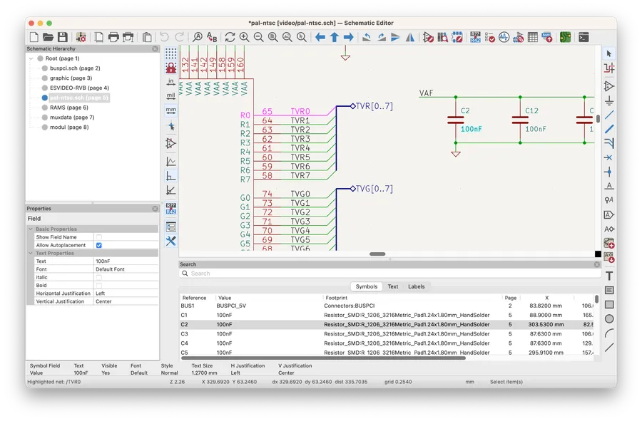
This module is used for creating and editing electronic schematics. It allows users to place components, wire them together, and annotate the design, providing the logical foundation for the subsequent PCB layout. - PCB Editor (Pcbnew)
This is the heart of KiCad for physical layout, where components from the schematic are placed and connected via traces, creating the actual PCB design. Formerly known as PCBNew, it facilitates complex routing, component placement, and board management. - Gerber Viewer
This tool allows users to view and inspect Gerber files, which are the standard output for manufacturing PCBs, ensuring the design can be accurately produced. This feature is crucial for verification before sending the files to a manufacturer. - Symbol Editor
This module is used for creating and modifying symbols for the schematic editor, allowing you to create or adjust symbols to match the components being used in your design. - Footprint Editor
This powerful tool allows you to create and modify footprints of your components for use in the PCB editor. Accurate footprints ensure the correct physical placement of components on the board. - Project Manager
This is a central module where you manage your design projects. It consolidates all the schematics, layout files, and project settings into a single working environment, facilitating an organized workflow.
These modules are designed to work together seamlessly, from the initial schematic design to the final manufacturing files. The schematic defines the connectivity of the electronic circuit, the PCB editor translates this into a physical board layout, and the Gerber viewer is a critical last step in verifying that what you have designed will be properly manufactured. KiCad's integrated approach ensures a streamlined design workflow and reduces the likelihood of errors.
Setting Up KiCad for Your First Project
Initiating your PCB design journey with KiCad requires a proper setup, which involves downloading, installing, and configuring the software to align with your specific requirements. This process also includes the crucial step of setting up the necessary component libraries.
- Downloading KiCad
Visit the official KiCad website and download the appropriate installer for your operating system (Windows, macOS, or Linux). Ensure you select the latest stable release to benefit from the most recent features and bug fixes. Download links are typically found in the 'Download' or 'Get KiCad' section of the website. - Installing KiCad
Run the downloaded installer and follow the on-screen instructions. On Windows, the installer typically offers an option to choose installation location. On macOS, drag the KiCad application to your Applications folder. For Linux users, the installation process may vary based on distribution, commonly using package managers such as apt or yum. - Initial Configuration
After installation, KiCad should be launched. Upon first use, KiCad may prompt you to select a language, or configure some paths, ensure you have selected your region. These configuration include setting up project paths, and other preference settings. It's also good practice to configure the theme according to your preference. - Setting Up Component Libraries
KiCad's component libraries are essential for placing parts on your schematics and PCBs. KiCad includes a standard set of libraries. Additionally, you can add external libraries from various sources on github, and configure the library paths within KiCad to enable easy access to necessary components.
| Task | Description | Key Action |
|---|---|---|
| Download | Acquire the KiCad software | Navigate to the official KiCad website and select your OS installer. |
| Installation | Install KiCad on your machine | Run the downloaded installer and follow on-screen prompts. |
| Initial Configuration | Configure initial settings | Launch KiCad and set project paths and language preferences. |
| Library Setup | Configure necessary component libraries | Add local or github based component libraries and set the necessary paths |
Schematic Capture: Building Your Electronic Blueprint
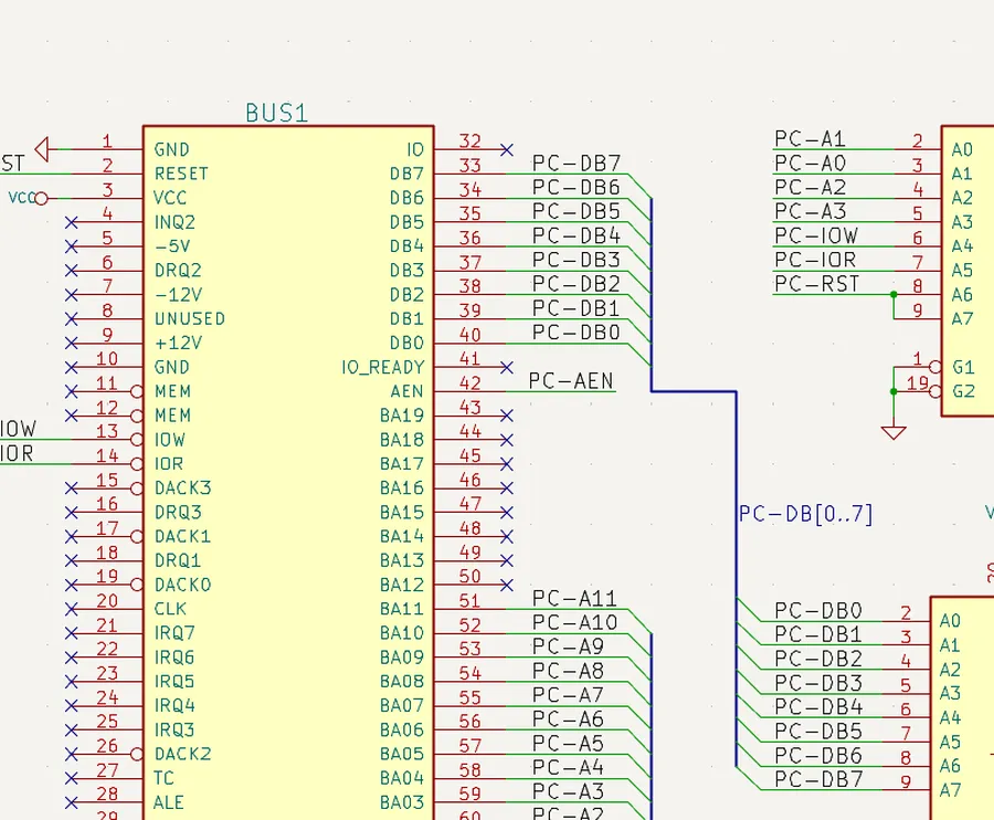
Schematic capture in KiCad is the essential first step in PCB design, where you create a graphical representation of your electronic circuit. This process involves selecting components, placing them logically, and wiring them together to define the electrical connections, ultimately forming the basis for your printed circuit board layout. The schematic serves as a blueprint, ensuring a clear understanding of the circuit before moving onto physical implementation.
- Component Placement
Begin by strategically placing electronic components from KiCad's extensive libraries onto your schematic canvas. Group related components logically, facilitating easier schematic reading and subsequent layout. - Wiring and Connections
Draw wires connecting component pins according to your circuit design. KiCad provides tools for easy wire routing and labeling. Ensure all connections are accurately established to reflect the intended circuit operation. - Annotation and Labeling
Label components with unique reference designators (e.g., R1, C2, U3), enhancing readability and traceability. Proper annotation aids in both the design phase and later debugging and manufacturing stages. - Hierarchical Schematics
Employ hierarchical schematics for complex designs, dividing circuits into manageable sub-blocks. This method promotes modular design and enhances reusability. KiCad supports creating hierarchical sheets to organize complex systems. - Net Names
Assign net names to wires, allowing you to reference them consistently, especially when dealing with connections across different parts of the schematic. Properly named nets improve clarity and facilitate design verification.
By meticulously creating a clear and accurate schematic, you lay the groundwork for a successful PCB design. The information within this schematic, such as component interconnections, net names, and component values are crucial to creating a reliable PCB layout in the next step.
Transitioning from Schematic to PCB Layout
The transition from a completed schematic to a physical PCB layout is a critical stage in the KiCad design process. This involves converting the logical connections and component placements defined in the schematic into a physical arrangement on a printed circuit board, using the PCB editor. This stage is paramount for ensuring the manufacturability and functionality of the final PCB.
This transition focuses on several key steps. First, importing the netlist created from the schematic. This netlist provides the connectivity information for all components. Second, correctly placing the components on the PCB board outline, which will define the physical space constraints. Third, setting up the board layers, which is crucial for multilayer PCBs. This sets the stage for the subsequent routing of traces.
The accuracy of this transition is paramount. Any inaccuracies in importing the netlist or misplacement of the components can have serious implications on the manufacturability or the functionality of the final product. Therefore, careful consideration is needed when setting up your board and its parameters. Let's take a look at the typical process of completing this step.
- Generate the Netlist from the Schematic
After completing and verifying your schematic, the first step is to generate a netlist file. This file acts as a bridge between the schematic editor and the PCB editor, conveying the connection information of the components. Within the schematic editor, you can create a netlist using 'Tools' -> 'Generate Netlist' (or equivalent). Select the appropriate netlist format, such as the commonly used 'KiCad netlist' format. - Create a New PCB File
If you have an existing PCB file, open it. If starting from scratch, use File -> New -> PCB. This will launch the PCB editor, presenting a blank board layout. You may need to configure the board dimensions, typically done in the 'Page Layout' tool or via 'File' -> 'Board Setup' (or equivalent). - Import the Netlist to PCB Editor
In the PCB editor, use 'Tools' -> 'Update PCB from Schematic' (or equivalent) and choose the netlist file created earlier. KiCad then reads the file and places all of the components onto the board, normally outside of the board area. You can modify the PCB board area by selecting File -> Board Setup -> Board area and modify the appropriate parameters. You may need to set the component locations so that they don't overlap, by using the 'Move' tool to drag components from the default placement off the PCB, and onto the PCB. - Arrange components within PCB
Arrange components within the board area. Consider the functionality of your circuit and placement guidelines when placing the components. For example, decoupling capacitors should be placed close to the power pins of chips, and components that are electrically connected should be placed near each other to reduce trace lengths. - Define Board Layers
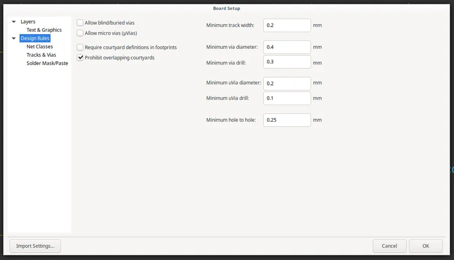
Set up the necessary layers in the layer manager. Typical PCB designs use at least two layers (top and bottom), and more complex boards can use multiple layers, such as internal power and ground planes. This is done through 'File' -> 'Board Setup' -> 'Layers' (or equivalent). Define all layer types and any stackup information.
Mastering PCB Layout: Key Techniques and Tips
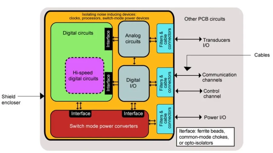
Effective PCB layout is critical for ensuring the functionality, reliability, and manufacturability of electronic devices. This section delves into essential techniques for routing traces, managing vias, creating custom footprints, and adhering to design rules within KiCad, focusing on optimizing for performance and minimizing potential issues.
Key aspects of mastering PCB layout include:
- Trace Routing Strategies
Efficient trace routing minimizes signal interference and ensures proper signal integrity. Key considerations include maintaining consistent trace widths, minimizing trace lengths, and employing techniques like differential routing for high-speed signals. - Via Management
Vias are used to connect traces between different layers. Proper via management is essential to minimize impedance discontinuities and ensure reliable connections. Techniques include using appropriate via sizes and spacing, and avoiding vias in critical signal paths where possible. - Custom Footprint Creation
Creating custom footprints for components not available in the standard library is a crucial skill. A well-designed footprint ensures proper component mounting and solderability, adhering to manufacturer specifications and tolerances is paramount. - Design Rule Checking (DRC)
KiCad's built-in Design Rule Checker is vital for verifying compliance with manufacturing constraints and design best practices. Setting up appropriate DRC rules ensures that the final PCB layout is free from common errors like trace spacing violations and drill hole proximity problems.
| Technique | Description | Benefits |
|---|---|---|
| Differential Routing | Routing two traces as a pair to carry differential signals | Reduces noise and improves signal integrity, especially for high-speed signals. |
| Power Plane Considerations | Use of dedicated layers for power and ground | Reduces impedance, minimizes noise and improves power distribution. |
| Via Stitching | Using multiple vias to connect ground planes on different layers | Minimizes inductance and improves ground integrity. |
3D Visualization and Design Checks
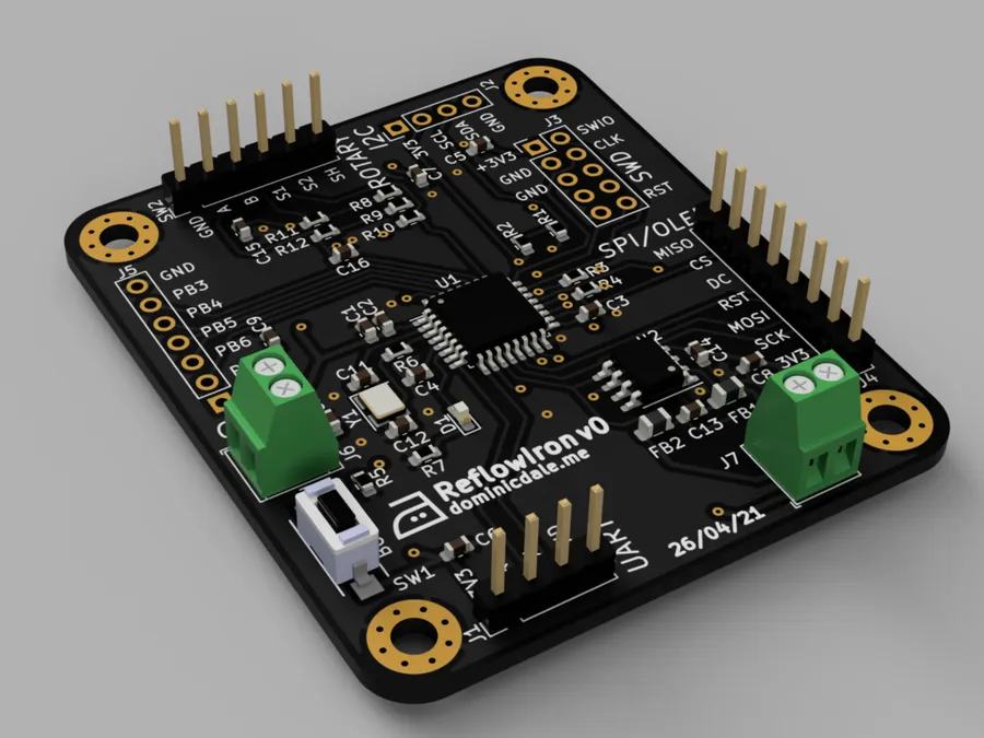
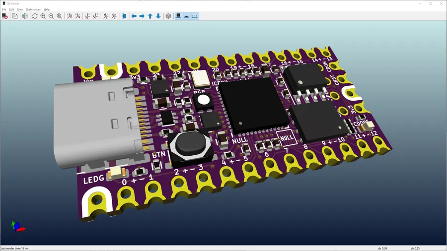
KiCad's 3D Viewer is an invaluable tool for ensuring the mechanical integrity of your PCB design, allowing for a visual inspection of component placement and potential interferences before manufacturing. Complementing this, the Design Rule Check (DRC) functionality is crucial for identifying design errors that could lead to manufacturing defects or performance issues.
The combined use of 3D visualization and DRC tools in KiCad is essential for efficient PCB design and manufacturing, facilitating early detection of design flaws, thus reducing costly re-spins.
- 3D Viewer Functionality
The 3D viewer allows you to visualize your PCB layout with components rendered in three dimensions. This is critical for detecting mechanical interferences, assessing component clearances, and ensuring the overall fit of the designed PCB within its intended enclosure. The 3D model representation helps in the early identification of issues related to component height and placement. - Benefits of 3D Visualization
The 3D viewer offers a precise representation of the board in a way that 2D views cannot. It helps identify misalignments, potential for short circuits caused by mechanical interference, and the correct positioning of components within the enclosure. The ability to see the entire assembly makes design reviews much more effective. - Design Rule Check (DRC) Functionality
The DRC feature in KiCad automatically checks your PCB layout against a set of predefined rules, including trace widths, clearances between traces and pads, via sizes, and more. This functionality is crucial for ensuring that your design adheres to industry standards and manufacturing requirements. - Importance of DRC Checks
Running a DRC check at various stages of the PCB design process can significantly minimize the risk of manufacturing errors. DRC violations are flagged early, enabling design corrections before the manufacturing stage, which reduces costs and delays. - Configuring DRC Rules
KiCad allows users to customize DRC rules based on their specific needs and the requirements of the chosen PCB manufacturer. This flexibility ensures that designs comply with specific manufacturing constraints, improving the design’s success rate.
Generating Gerber Files for PCB Manufacturing
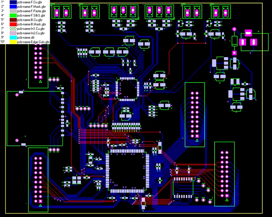
The culmination of PCB design in KiCad involves generating Gerber files and drill files, which are essential for PCB fabrication. These files communicate the precise layout and specifications of your board to the manufacturer. This section outlines the process of creating these files and selecting a suitable PCB manufacturer.
- Accessing the Plotting Function
Open the PCB layout in KiCad's PCB editor. Navigate to 'File' and select 'Plot' to open the plotting dialog. - Configuring Gerber Output
In the Plot dialog, select 'Gerber' as the plot format. Choose the directory where you wish to save the output files. This location should be easily accessible. Select the layers you wish to output. Typically, this includes copper layers (top and bottom), silkscreen layers, solder mask layers, and the board outline. Ensure that the layer selection reflects the full scope of your design's needs. - Configuring Drill File Output
Within the same Plot dialog, select the 'Generate Drill Files' option. Choose the output directory for the drill files. Set the drill file format based on your manufacturer's requirements (Excellon format is commonly used). Also specify the units (inches or millimeters) for the drills and consider whether to use 'plated thru holes only' when applicable. - Generating the Files
Click the 'Plot' button to generate the Gerber files. After this is complete, click on 'Generate Drill File' to create the drill files. This process creates a series of files (.gbr, .drl) required for board fabrication. Inspect these files using Gerber viewer to confirm accuracy. - Selecting a PCB Manufacturer
When choosing a PCB manufacturer, consider factors like cost, fabrication time, material capabilities, and minimum order quantity. Compare different manufacturers based on their offerings and capabilities, as it is critical to select a manufacturer that can meet the specific requirements of your project. Ensure the manufacturer is capable of handling your board's layer count, trace width, and other critical specifications. - Uploading Files to Manufacturer
Carefully review the Gerber and drill files before uploading them to your chosen PCB manufacturer. Most manufacturers have their own online portals for file upload. Ensure that files are uploaded to the correct location. Double check all files to be sure they have been uploaded correctly. - Confirm Manufacturing Details
Prior to manufacturing, confirm with the manufacturer any specific details such as material choice, surface finish, and any assembly requirements. Clear communication with the manufacturer will streamline the process and mitigate delays and errors.
Frequently Asked Questions about KiCad PCB Design
This section addresses common queries regarding KiCad PCB design, offering insights into its capabilities, limitations, and comparisons with other Electronic Design Automation (EDA) tools, specifically focusing on user concerns about cost, complexity, and usability.
- What is the role of a PCB in KiCad?
In KiCad, the PCB, or Printed Circuit Board, represents the physical layout of your electronic circuit. It is the medium upon which electronic components are mounted and interconnected via conductive traces, effectively translating the schematic diagram into a manufacturable physical form. KiCad's PCB editor allows for component placement, trace routing, and design rule verification. - Is KiCad truly free for all users?
Yes, KiCad is completely free and open-source software. It is licensed under the GNU General Public License, meaning there are no costs associated with its use, modification, or distribution. This eliminates the financial barrier often encountered with commercial EDA software, making it an accessible tool for hobbyists, educators, and professional engineers alike. - What are some common disadvantages associated with using KiCad?
While KiCad is a powerful tool, some common disadvantages include a steeper learning curve for beginners compared to some other software, potentially less readily available support compared to commercial offerings, and sometimes a need for third-party plugins to enhance specific functionalities or features. It is essential to consider these factors when deciding whether KiCad fits your requirements and resources. - How does KiCad compare with Eagle in terms of user-friendliness?
The user-friendliness of KiCad versus Eagle is subjective and often dependent on individual preferences and prior experience. While some users find KiCad's interface more modern and intuitive, others may prefer the more established layout of Eagle. Generally, both tools are complex and require time and dedicated practice to master effectively. KiCad’s large and active community provides a significant amount of learning resources. - Where can I find KiCad PCB design examples?
KiCad PCB design examples can be found in the official KiCad documentation, open-source hardware repositories (e.g., GitHub), various online forums dedicated to KiCad usage, and through community-driven tutorials. These examples provide excellent practical guidance for various levels, from basic to advanced designs. - How to use KiCad for professional PCB design?
KiCad is used in a professional setting, and it can be used to design a wide range of PCBs. The professional workflow includes rigorous version control practices, utilizing advanced features such as scripting and customization, adhering to industry standard design rules, and performing in-depth analysis and verification before manufacturing. Professional usage also encompasses the development of specific component libraries that meet the company's standards. - What about online KiCad tutorials?
There are many high quality online tutorials available for KiCad. They range from beginner to advanced and cover different aspects of using the tool, such as creating schematic diagrams, PCB routing, library management, design rule checking, and 3D visualization. There are both text and video based tutorials available.
Advanced KiCad Features and Workflows
KiCad, while powerful out-of-the-box, extends its capabilities through advanced features like scripting with Python and the use of plugins, alongside refined workflows that greatly enhance design efficiency. These tools and methods are essential for power users and complex PCB designs. This section delves into these capabilities, focusing on automation and customization.
- Scripting with Python in KiCad
KiCad's API allows Python scripting to automate tasks, manipulate board data, and add custom features. This includes batch processing, DRC modifications, and other advanced functionalities. - Utilizing Plugins for Enhanced Functionality
Plugins, often written in Python, extend KiCad with specific features, from importing specific data formats to advanced analysis. The plugin ecosystem continually expands, offering solutions for niche requirements. - Creating Custom Footprints and 3D Models
KiCad enables the design of custom footprints and integration of 3D models for components. This allows more accurate representation and aids in visualization during the design phase. These custom assets ensure compatibility and optimal component placement. - Streamlining Design Workflows
Establishing a consistent and efficient design workflow is vital, especially for large or intricate PCB designs. This includes templating designs, setting up standardized design rule sets, and using version control systems for collaboration and design iteration tracking.
| Feature | Description | Benefits |
|---|---|---|
| Python Scripting | Automates repetitive tasks using the KiCad API. | Reduces manual labor and potential for errors; accelerates the design process. |
| Plugin Integration | Adds specific functionalities and integrations to KiCad. | Extends KiCad's capabilities for niche needs; integrates with other tools. |
| Custom Footprint Creation | Allows the user to design footprints for unique components. | Ensures accurate representation in the PCB layout; improves design compatibility. |
| Workflow Optimization | Establishes structured design procedures. | Enhances efficiency and collaboration; maintains consistency across projects. |
Troubleshooting Common KiCad PCB Design Issues
Encountering issues during PCB design with KiCad is a common part of the learning process. This section provides guidance on diagnosing and resolving typical problems, ensuring a smoother design experience. Addressing issues early in the design process can save significant time and resources.
- Incorrect Footprints
A common problem is using the wrong footprint for a component, which leads to physical incompatibility. Always double-check component datasheets against the KiCad library before placing components. If an incorrect footprint is used, modify or create a new footprint and replace it in the schematic and PCB editor. - DRC Errors
Design Rule Check (DRC) errors often indicate spacing issues, short circuits, or trace width violations. Carefully review the DRC report, understand each error and make necessary adjustments to the PCB layout. Properly setting up design rules and constraints in KiCad will minimize these errors. - Netlist Import Issues
Problems during netlist import, can occur due to discrepancies between schematic symbols and PCB footprints. When this occurs, double-check that the symbols and footprints are correctly linked, and verify that all components from the schematic have footprints assigned. Check that all the libraries being used are properly configured to prevent import issues. - Routing Challenges
Complex routing involving dense layouts can lead to challenges, like hard-to-route connections. Techniques such as utilizing multiple layers, optimizing component placement, and using vias effectively can ease complex routing issues. Sometimes, small changes to component positions can significantly improve routing efficiency. - Gerber File Generation Errors
Issues during Gerber file generation are usually due to incomplete setup or incorrect selections of layers. Carefully review your layers selection, the output options, and make sure you are exporting the appropriate files for your board manufacturer.
KiCad PCB design offers a powerful, free platform for creating custom circuit boards. This guide has explored the core elements, from setting up your project to generating manufacturing files. By mastering KiCad, you gain the ability to transform your electronic concepts into tangible realities, fostering innovation and learning. Embrace the power of KiCad to take your projects from schematic to physical reality, pushing the boundaries of your technical skills and engineering possibilities.