Mastering Board Design: From Concept to Creation
In today's interconnected world, board design is fundamental, from the aesthetic arrangement of a mood board to the intricate circuitry of a PCB. This article will guide you through the various aspects of board design, exploring its creative and technical facets, equipping you with knowledge to tackle any board design challenge and create high-quality, functional and visually appealing designs.
Understanding Different Types of Board Design
Board design encompasses a wide spectrum of applications, ranging from purely aesthetic and inspirational tools to highly complex electronic circuit boards. This section explores the diverse types of board designs, each serving distinct purposes and requiring different materials and techniques. Understanding these differences is crucial for choosing the right approach for any project.
The following is a brief overview of three prominent types of board designs:
- Mood Boards
Primarily used in creative fields like design, fashion, and advertising, mood boards are collages of images, colors, textures, and text that express a particular aesthetic or feeling. They serve as a visual reference for the direction of a project. Materials include physical boards (cork, foam), paper, magazines, fabric swatches, or digital tools. - Bulletin Boards
Designed for communication and information sharing, bulletin boards are commonly found in offices, schools, and public spaces. They display announcements, notices, and other timely information. Materials typically include cork or fabric surfaces, push pins, and sometimes enclosed glass cases. - Printed Circuit Boards (PCBs)
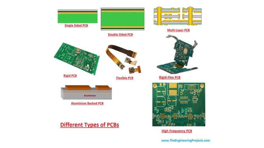
At the core of most electronic devices, PCBs are boards that mechanically support and electrically connect electronic components. They are made from materials like fiberglass with copper traces for electrical conductivity and use advanced techniques to manufacture. They are essential in anything from simple circuits to complex computing platforms.
Mood Board Design: Gathering Inspiration
Mood board design is a fundamental step in any creative project, acting as a visual tool to explore and define the project's aesthetic direction. It involves gathering a curated selection of images, colors, textures, and other elements that resonate with the project's theme, providing a tangible representation of the intended feel and style. This process is crucial for ensuring that all design choices remain aligned and contribute to a cohesive final product.
- Physical Mood Boards
Physical mood boards involve tangible materials like printed images, fabric swatches, and paint chips, offering a tactile and interactive experience. They allow for flexible arrangements and the ability to physically feel textures. Key to consider when creating physical mood boards include the selection of a board (foam core, cork board or a large sheet of paper), how the materials are attached (pins, glue, tape) and how to arrange them to create a visually appealing and informative board. - Digital Mood Boards
Digital mood boards utilize software and online platforms to assemble images and elements. They are easily shareable, editable, and can be more cost-effective than physical boards. Digital mood boards also offer a wider range of sources for inspiration, easily capturing and organizing images, colors, and links online. Some popular digital tools include Pinterest, Milanote, and Adobe Creative Cloud applications.
| Feature | Physical Mood Boards | Digital Mood Boards |
|---|---|---|
| Material Tactility | High (direct physical interaction) | Low (visual interaction only) |
| Shareability | Requires physical transport or photography | Easily shared online |
| Editability | Requires physical rearranging, can be time consuming | Easily and quickly edited |
| Cost | Can involve costs of print materials | Often free or subscription based |
| Source of Inspiration | Limited to physical materials | Wide range, includes images, links, videos |
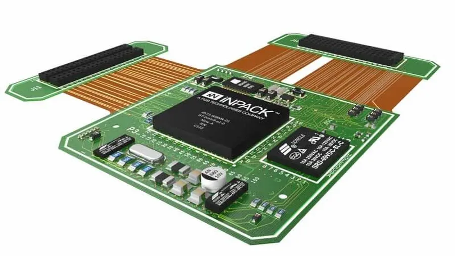
PCB Design Fundamentals: From Schematic to Layout
Printed circuit board (PCB) design is the cornerstone of electronic hardware development, translating abstract circuit diagrams into physical layouts. This process encompasses several crucial stages: schematic capture, component placement, routing, and design rule checking, all working in concert to produce a reliable, manufacturable product.
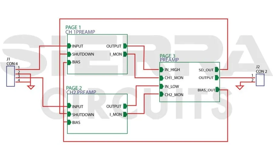
- Schematic Capture
The initial step involves creating a logical representation of the circuit using schematic capture software. This includes selecting electronic components from libraries and wiring them together according to the design's functional intent. The schematic is not concerned with physical dimensions but rather with the electrical interconnections between components. - Component Placement
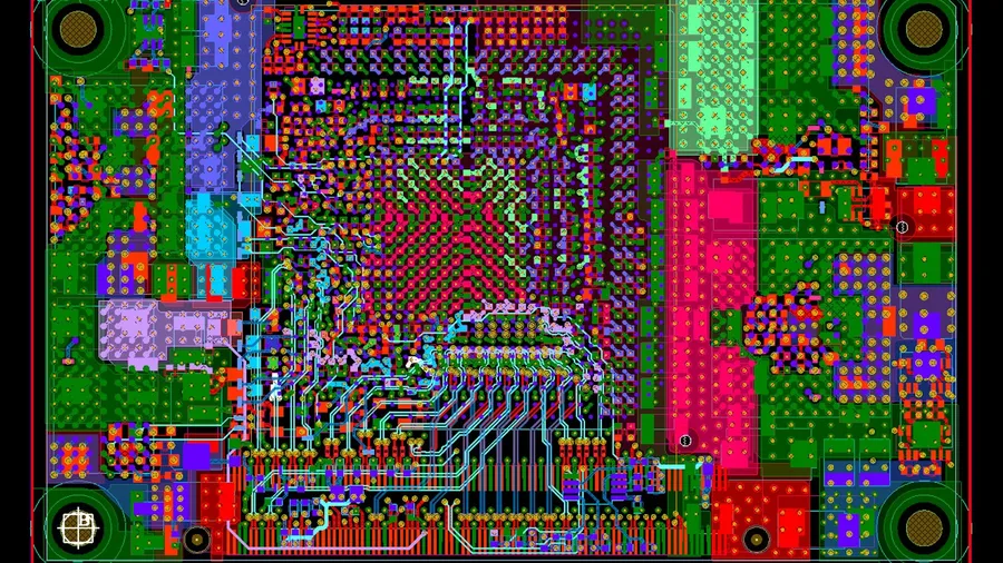
Once the schematic is complete, the physical placement of components on the PCB is planned. This stage takes into account thermal management, signal integrity, and manufacturing constraints. It's a balancing act between minimizing circuit footprint and ensuring optimal electrical performance. - Routing
Routing refers to the process of creating copper traces on the PCB to connect components according to the schematic. This critical step determines the electrical pathways and requires careful consideration of trace width, spacing, and layer assignments, to achieve specific impedance, reduce crosstalk, and ensure signal integrity. - Design Rule Checking (DRC)
DRC is a critical automated process that verifies the PCB layout against predefined design rules, covering aspects like trace widths, clearances, and component spacing. It acts as a safeguard, detecting potential manufacturing problems before the board is fabricated, saving time and costs.
| Stage | Description | Key Considerations |
|---|---|---|
| Schematic Capture | Creating a logical representation of the circuit. | Component selection, wiring connections. |
| Component Placement | Positioning components on the physical board. | Thermal management, signal integrity, manufacturability. |
| Routing | Creating conductive pathways to connect components. | Trace width, spacing, layer assignment, impedance. |
| Design Rule Checking | Automated verification of layout against design rules. | Trace widths, clearances, component spacing, manufacturability. |
Essential Tools for PCB Design
The selection of appropriate software is crucial for successful Printed Circuit Board (PCB) design. This section introduces popular Electronic Design Automation (EDA) software and platforms used in the industry, comparing their features, pricing models, and suitability for different project needs.
| Tool | Pricing | Key Features | Pros | Cons | Suitable For |
|---|---|---|---|---|---|
| CircuitMaker | Free | Schematic capture, PCB layout, community-based | Cloud-based, easy to use, free | Limited advanced features, requires internet connection | Hobbyists, educators, and small projects |
| EasyEDA | Free (with paid options) | Schematic capture, PCB layout, SPICE simulation | Browser-based, user-friendly, integrated component library | Some limitations on complex designs, dependent on internet access | Small to medium-sized projects, prototyping |
| Cadence Allegro | Commercial (high cost) | Advanced schematic, layout, signal integrity analysis | Industry-standard, powerful, extensive features | High cost, steep learning curve | Large and complex projects, high-performance applications |
| Altium Designer | Commercial (mid-high cost) | Schematic capture, PCB layout, 3D visualization, collaboration tools | Robust, versatile, comprehensive feature set | Higher cost, needs strong hardware | Professional designs, complex projects |
| KiCad | Free, Open source | Schematic Capture, PCB layout, 3D viewer | Highly customizable, cross platform, free | Can be complex for beginners, requires time to master | All types of projects, personal to professional |
Step-by-Step Guide to Creating a Digital Design Board
Creating a digital design board is a crucial step in visualizing and communicating your design ideas effectively. This process involves sourcing, editing, and arranging images and other elements to form a cohesive and visually compelling presentation. The goal is to create a digital space that encapsulates the essence of your design concept.
- 1. Define Your Board's Purpose
Begin by identifying the primary objective of your design board. Are you creating a mood board for a branding project, a concept board for a product design, or a vision board for a room makeover? Clearly defining the purpose will guide your selection of images, colors, and other elements. - 2. Gather Relevant Visual Assets
Collect images, illustrations, color swatches, and texture samples that align with your project’s theme and style. Use a variety of sources, such as design inspiration websites, stock photo libraries, and your own photography. Ensure that the quality of the images is suitable for digital viewing. - 3. Choose a Digital Platform
Select an appropriate platform for creating your digital board. Options include dedicated design software like Canva, Adobe Illustrator, or Figma; productivity tools like Google Slides or PowerPoint; or online collaboration tools like Miro or Mural. Consider factors such as ease of use, available features, and accessibility. - 4. Image Editing and Preparation
Before arranging images on your board, edit them as needed. This may include cropping, resizing, adjusting colors, or removing backgrounds. Consistent image sizes and quality will result in a professional-looking board. Tools like Photoshop, GIMP, or online image editors can be used for this purpose. - 5. Arrange and Organize Elements
Arrange your images, colors, and other elements on your chosen platform. Consider the visual hierarchy and flow of your board, placing key elements in prominent positions. Group similar elements to maintain a cohesive and organized appearance. Experiment with different layouts until you achieve the desired visual balance and impact. - 6. Add Text and Annotations
Use text boxes or annotations to add descriptive notes, keywords, and explanatory text to your board. This helps to communicate specific details and provide context for the visual elements. Choose a legible font and appropriate text size that complements the overall design. - 7. Review and Iterate
Take a step back and review your digital design board. Are the key elements clearly communicated? Is the visual layout cohesive and compelling? Are there any adjustments that need to be made? Be prepared to iterate and make refinements as needed to achieve your desired outcome. - 8. Share and Collaborate
Once you are satisfied with your design board, share it with your team, clients, or stakeholders for feedback and collaboration. Most digital platforms offer options for sharing via email, links, or collaborative workspaces. Encourage open feedback and use it to further refine your design process.
PCB Design for Different Applications
The requirements for Printed Circuit Board (PCB) design vary significantly based on the intended application. High-speed circuits, low-power devices, and Radio Frequency (RF) applications each present unique challenges that necessitate tailored design and layout strategies to ensure optimal performance and reliability. Understanding these application-specific needs is paramount for effective PCB design.
| Application | Key Design Considerations | Layout Priorities | Material Considerations |
|---|---|---|---|
| High-Speed Circuits | Controlled impedance, signal integrity, crosstalk minimization | Short trace lengths, matched impedance, proper termination | Low-loss dielectrics, tight impedance control, minimal signal reflections |
| Low-Power Devices | Power efficiency, minimal current leakage, component selection | Efficient power distribution, optimized component placement, power plane design | Low-current leakage materials, optimized thermal vias |
| RF Applications | Antenna matching, impedance control, signal integrity, low noise | Precise impedance matching, minimized parasitic capacitance/inductance, shielding | Low-loss dielectrics, materials with stable dielectric constant, surface finish for high frequency |
Board Design Best Practices for Manufacturability
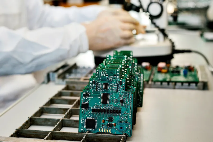
Design for Manufacturability (DFM) in PCB design is crucial for ensuring that a circuit board can be produced efficiently, reliably, and cost-effectively. Implementing DFM practices avoids common pitfalls that can lead to production delays, increased costs, and reduced yields. This involves a series of design considerations that begin early in the design process.
| Design Aspect | Best Practice | Impact on Manufacturability |
|---|---|---|
| Component Spacing | Maintain adequate spacing between components based on the manufacturer's specifications. | Prevents interference during placement and assembly, reducing the risk of shorts and misalignments. |
| Trace Widths and Spacing | Use appropriate trace widths and spacing based on current requirements and impedance matching needs. | Ensures reliable signal transmission, avoids impedance issues, and supports proper etching. |
| Via Placement | Place vias strategically to avoid component areas, particularly beneath surface mount components. | Ensures reliable soldering of components, reduces issues with solder bridging and increases yield rates. |
| Solder Pad Design | Design solder pads that meet the specifications for component footprints, with appropriate spacing and alignment. | Enables correct component placement and prevents tombstoning, which results in efficient automated assembly processes. |
| Panelization | Plan board layouts to be manufactured as a panel with standardized panel borders and fiducials. | Optimizes material use and the efficiency of automated assembly and handling. |
| Gerber Files | Generate all necessary Gerber files, including drill files, with high precision and correct dimensions and format. | Provides manufacturing partners with the data needed to produce the PCBs accurately. |
| Silkscreen Layer | Include a clear and readable silkscreen layer that contains component labels and pin-1 identification. | Facilitates easier component population and reduces errors in assembly. |
Frequently Asked Questions about Board Design
This section addresses common questions regarding board design, encompassing various aspects from fundamental concepts to practical applications, aiming to clarify the nuances of creating effective board designs across different disciplines.
- What is the fundamental difference between board-level design and IC (integrated circuit) design?
Board-level design involves arranging and connecting various components (including ICs) on a printed circuit board to achieve a specific electronic function, focusing on system-level integration. IC design, conversely, focuses on creating the intricate circuitry within an individual chip (IC), involving transistor-level design, fabrication, and optimization for performance and density. Board design utilizes existing ICs as building blocks, while IC design creates those building blocks. - How can I create a free design board for project planning?
Several free digital tools can facilitate the creation of a design board. For example, online platforms like Miro, Trello, and Canva allow users to compile images, text, and other visual elements to conceptualize their ideas. Consider using a digital document or presentation software for a simple free option, too, where you can insert and organize text, images, and shapes. Physical boards can also be constructed using cardboard and glue if preferred, and all you need is access to visual materials to cut out and arrange. - What are the key steps in creating a physical board design for a creative project?
Creating a physical design board involves several steps. First, gather all your materials like images, fabric swatches, and color samples. Then, arrange these materials on your board. Start with a main focal point, then build around it to see how the elements compliment each other, securing them with pins or glue. Then, evaluate the overall feel of your design, make alterations, and keep adding or taking away elements to reach your desired outcome. - How can I effectively use a board to gather and organize my ideas?
Use the board to capture your thought process, by visually representing different aspects of your project. Begin by placing a central idea or theme. Then, add supporting ideas, images, and related notes surrounding it. Organize these elements in a logical flow to illustrate the connections between each concept. Regularly revisit and update the board as your ideas evolve to keep your vision clear. - Are there any free software tools available for PCB design, and what are their limitations?
Yes, numerous free PCB design software options are available, such as KiCad and EasyEDA. While these are capable for many projects, they might have limitations compared to commercial software like Altium Designer or Cadence Allegro. Limitations might include a smaller component library, less advanced simulation capabilities, and less community support for specific complex design challenges. These limitations are acceptable for hobbyist or simple to moderate design projects, but may be too limiting for large complex or industrial-grade projects. - What is the typical workflow for PCB design, from concept to manufacturing?
The typical workflow begins with defining the project requirements, then schematic capture, component selection, and PCB layout planning. After placement and routing, a thorough design rule check and verification is conducted. The final stage is generating manufacturing files (Gerber files), BOMs, and assembly drawings, ensuring the designs are ready for mass production. Iterative processes are often employed for optimizing designs before manufacturing. - What are the most common pitfalls to avoid in board design?
Common pitfalls include improper component spacing that impedes soldering, traces that are too narrow for the intended current, insufficient thermal management for high-power components, and lack of a thorough Design for Manufacturability review. Additionally, neglecting to verify the correct pin assignment of components and not having clear labels on parts are other errors that should be avoided by proper planning and review.
Advanced Techniques in PCB Board Design
Modern high-performance and specialized electronic applications demand advanced techniques in PCB design. These techniques extend beyond basic single-layer layouts and include strategies for managing signal integrity, heat dissipation, and increased circuit density, crucial for meeting the rigorous demands of advanced systems.
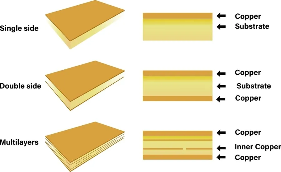
- Multilayer PCBs
Multilayer PCBs provide increased circuit density by allowing traces on multiple layers, which can be interconnected using vias. This is essential for complex designs with high component counts and intricate routing requirements. - Impedance Matching
Impedance matching ensures that the signal power is transferred efficiently with minimal reflection, crucial for high-speed digital and radio frequency circuits. This involves controlling trace widths and spacing to achieve desired impedance values. - Thermal Management
Efficient thermal management is critical to avoid component overheating which can lead to device failure. Techniques include using thermal vias, heat sinks, and careful component placement to manage heat effectively.
Mastering board design requires a blend of creativity and technical expertise. Whether you're crafting mood boards, creating a bulletin board or designing intricate PCBs, understanding the core principles and utilizing the right tools will be key to achieving success. By embracing both the art and science of board design, you can create innovative solutions that power the world around us, whether it’s a circuit board or other types of boards, its design remains crucial for success.