Mastering PCB Drawing: From Schematic to Layout
In our interconnected world, printed circuit boards (PCBs) are the unsung heroes powering everything from our smartphones to complex industrial machinery. The ability to create accurate and efficient PCB drawings is the foundation of effective electronic design. This article will guide you through the entire PCB drawing process, from initial schematics to final layout, offering expert insights and practical advice along the way, and exploring the tools and methodologies required to transform your ideas into tangible electronic circuits. The ability to read and design a pcb drawing is an essential step in the design process.
Understanding the Basics of PCB Drawing
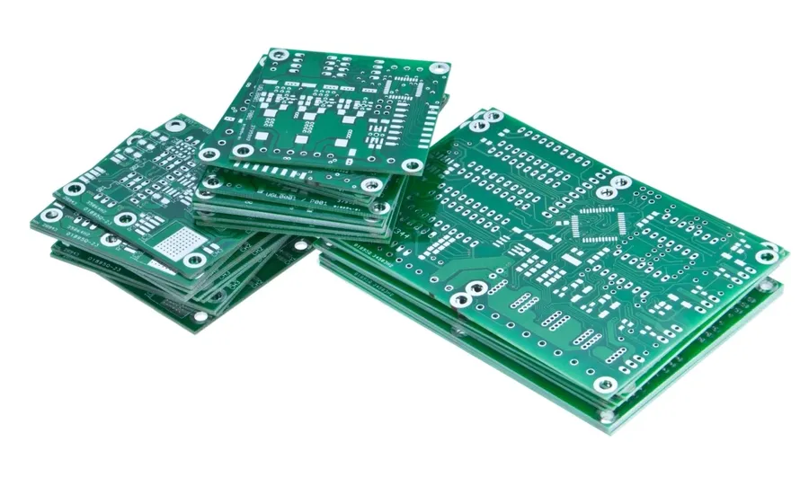
PCB drawing, at its core, is the process of creating detailed visual representations of a printed circuit board (PCB). These drawings serve as the fundamental blueprints for manufacturing electronic devices, encompassing various types such as schematics, layouts, and assembly drawings. Schematics detail the logical connections within an electronic circuit, while layouts translate these connections into a physical board design. Assembly drawings then guide the process of physically populating the board with components, thereby facilitating the entire product development lifecycle. These drawings are not merely graphical representations; they are the precise instructions that allow electronic products to be constructed to meet functional, performance, and quality specifications.
- Schematic Drawings
Represent the logical interconnection of electronic components. They use abstract symbols to depict electronic parts and their connections, focusing on the electrical functionality of the circuit rather than the physical layout. - Layout Drawings
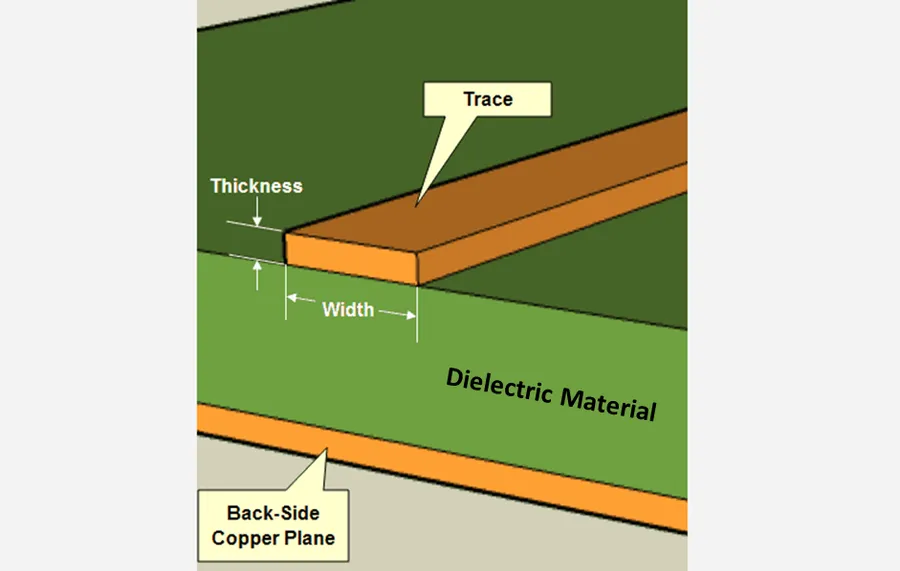
Show the physical arrangement of components on the PCB, including the traces (conductive paths), pads for soldering, and via locations. This drawing dictates how the electrical connections defined in the schematic are implemented on the physical board. - Assembly Drawings
Illustrate the placement and orientation of components on the PCB during the manufacturing and assembly phase. They provide critical information to guide the manual or automated placement process.
Schematic Capture: The Foundation of PCB Design
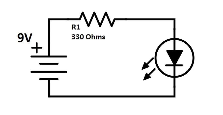
Schematic capture is the crucial first step in PCB design, representing the electronic circuit through a logical diagram. This process involves selecting appropriate symbols for electronic components, creating clear and organized diagrams, and drawing the necessary electrical connections using specialized software. The schematic serves as the blueprint for the subsequent physical layout of the printed circuit board.
- Component Symbol Selection
Choose symbols accurately reflecting the actual electronic components, adhering to established industry standards (e.g., IEEE 315). Consistent and accurate symbols are paramount for clarity and avoiding downstream errors. - Clear Diagram Organization
Employ a logical structure, arranging components for intuitive signal flow, placing related components near one another. This practice enhances readability and makes troubleshooting more efficient. - Electrical Connections
Draw connections (nets) between components using schematic capture tools. Ensure all interconnections match the desired circuit functionality, double checking for accuracy, and maintaining logical connections. - Pinout Management
Carefully assign pinouts of components according to datasheets, and follow this pinout when connecting nets. Incorrect pinout mapping can lead to incorrect circuit functionality. Consider the signal integrity impact of pinout assignments early in the schematic phase. - Signal Integrity
Consider signal path lengths at the schematic level to ensure optimal signal transfer. Use differential pairs if needed for noise reduction. Careful routing in the schematic phase can lead to less complicated and better performing boards.
The schematic diagram is not simply a drawing, it's the logical representation of how electrical signals flow through your design. It sets the stage for the physical PCB layout and is indispensable for effective PCB design, ensuring a seamless transition from conceptualization to the physical creation of the circuit board.
PCB Layout: Translating Schematics into Physical Boards
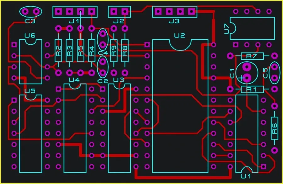
The transition from a schematic to a physical PCB layout is a crucial phase in electronic product development. This stage involves translating the logical representation of the circuit into a physical arrangement on the board, taking into account component placement, signal routing, and various physical constraints to ensure optimal performance and manufacturability.
Key considerations in PCB layout include optimizing component placement to minimize trace lengths and avoid signal interference, and effective trace routing that ensures signal integrity. Layer management is another critical factor, especially in multilayer PCBs, where careful planning is essential to achieve efficient routing and minimize the potential for signal degradation or crosstalk. Furthermore, thermal concerns, such as the placement of heat-generating components and the use of thermal vias, must be addressed to prevent overheating and ensure the reliable operation of the device.
- Component Placement
Strategic arrangement of components to reduce trace length and signal interference, considering thermal management and accessibility for manufacturing. - Trace Routing
Careful planning of conductive paths to maintain signal integrity, minimize noise, and adhere to impedance matching requirements. Avoiding sharp bends and unnecessary vias is crucial for high-speed signals. - Layer Management
Efficient use of multiple layers in multilayer boards to route signals, power, and ground, minimizing crosstalk and optimizing routing density. Stack-up design is key for impedance control. - Signal Integrity
Maintaining the quality of electrical signals throughout the board by using appropriate trace widths, spacing, and terminations. This is especially important for high-speed and high-frequency applications. - Thermal Management
Strategic placement of heat-generating components, utilizing heat sinks, thermal vias, and other techniques to dissipate heat effectively. - Manufacturing Considerations
Design for manufacturability (DFM) principles should be adopted, such as adequate spacing between components, fiducial marks for pick-and-place machines, and adherence to fabrication tolerances. This ensures smooth and cost-effective production processes.
| Aspect | Description | Importance |
|---|---|---|
| Component Placement | Arranging parts on the board | Affects signal paths and thermal performance |
| Trace Routing | Creating conductive pathways | Ensures signals reach intended destinations efficiently and without excessive noise |
| Layer Management | Organizing signal, power and ground layers in multi-layer PCBs | Reduces crosstalk and manages impedance |
| Signal Integrity | Ensuring signal quality | Prevents signal reflections and noise problems |
| Thermal Management | Addressing heat dissipation needs | Prevents component overheating and ensures reliability |
| Manufacturing | Designing for ease of assembly and fabrication | Reduces manufacturing defects and costs |
Essential PCB Design Tools and Software
Selecting the appropriate PCB design software is a critical step in the electronic design process. The right tool can significantly enhance productivity, streamline workflows, and reduce the likelihood of design errors. This section reviews popular software options, examining key features, pricing, and suitability for different design needs, to empower users in making informed decisions.
| Software | Key Features | Pricing | Strengths | Weaknesses | Platform |
|---|---|---|---|---|---|
| EasyEDA | Online editor, integrated schematic capture and PCB layout, cloud storage, vast component library | Free for basic use, paid plans for advanced features | Ease of use, accessibility, good community support, integrated PCB fabrication service | May lack some advanced features of high-end software | Online |
| CircuitMaker | Free professional-level PCB design software, collaborative, cloud based, integrated Altium library | Free | Professional-grade features at no cost, built in collaboration, component availability | Requires cloud dependence | Online |
| Autodesk EAGLE | Comprehensive schematic capture and PCB layout tools, powerful routing capabilities, integration with Fusion 360, large community support | Subscription-based | Robust features, powerful routing algorithms, strong integration with other Autodesk products | Can be costly for individual users, complex interface | Desktop |
| LibrePCB | Open source, cross-platform (Linux, macOS, Windows), modular design, customizable components | Free | Open source and free to use, cross platform, highly customizable | Smaller community compared to other options, may lack very advanced features | Desktop |
| KiCad | Open-source, cross-platform (Linux, macOS, Windows), feature-rich schematic capture and PCB layout, large and active community | Free | Feature-rich, free to use, good community support, highly customizable | Can have a steeper learning curve, less polished interface than paid options | Desktop |
| Cadence Allegro | High-end, professional PCB design suite, advanced routing, signal integrity analysis, team collaboration, for complex boards | High-cost subscription | Industry-standard for high-end designs, powerful analysis tools, excellent for large teams | Very costly, complex to learn and use, over kill for small projects. | Desktop |
When deciding between online and desktop software, consider your project needs and personal preferences. Online tools like EasyEDA and CircuitMaker provide accessibility and convenience, suitable for quick projects and collaborative environments, while Desktop solutions such as EAGLE, LibrePCB, KiCad and Cadence, which provide more in-depth features, ideal for complex projects that need full control and advanced functionality. The choice between open-source and proprietary software depends on your budget, the importance of customization, and community support.
Drawing PCB: Best Practices and Guidelines
Effective PCB drawing hinges on meticulous adherence to best practices that ensure both functionality and manufacturability. These guidelines encompass clear labeling, efficient layer usage, proper spacing, and adherence to design rules, all of which directly impact the performance, reliability, and ease of manufacturing of the final product. Prioritizing these principles reduces the likelihood of defects and increases design success.
- Component Labeling
Clearly label all components with their reference designators (e.g., R1, C2, U3). Use consistent naming conventions and ensure that labels are legible and do not overlap with other elements on the board. This aids in assembly, debugging, and future modifications. - Net Labeling
Label all important nets with descriptive names (e.g., VCC, GND, Clock). This clarity allows for easier identification of signal paths during layout and troubleshooting, ensuring signal integrity is maintained across the design. - Layer Management
Strategically assign different functions to each layer of a multi-layer board. Typically, power and ground planes are assigned to inner layers, while signals are routed on the top and bottom layers. This approach reduces electromagnetic interference and improves signal integrity. - Spacing and Clearances
Maintain proper spacing between traces and pads to prevent shorts and allow for adequate solder flow. Adhere to the design rules of your target manufacturing process (e.g., 6 mil trace width and spacing for standard processes, less than 4 mil for high density boards). Use design rule check (DRC) tools within your design software to verify these clearances and prevent issues. - Design Rule Checks (DRC)
Regularly run DRC checks throughout the design process. DRC tools identify violations of predefined rules, such as spacing violations, unconnected traces, and trace width limits. Early detection and correction of these errors significantly reduce risks of design defects. - Adherence to Manufacturing Tolerances
Incorporate manufacturing tolerances into the design process. Ensure that PCB traces and pad sizes are suitable for the chosen manufacturing method and materials, in order to prevent production difficulties. Adjust the PCB design according to the fabrication processes to minimize defects.
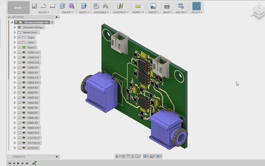
PCB Assembly Drawings and Documentation
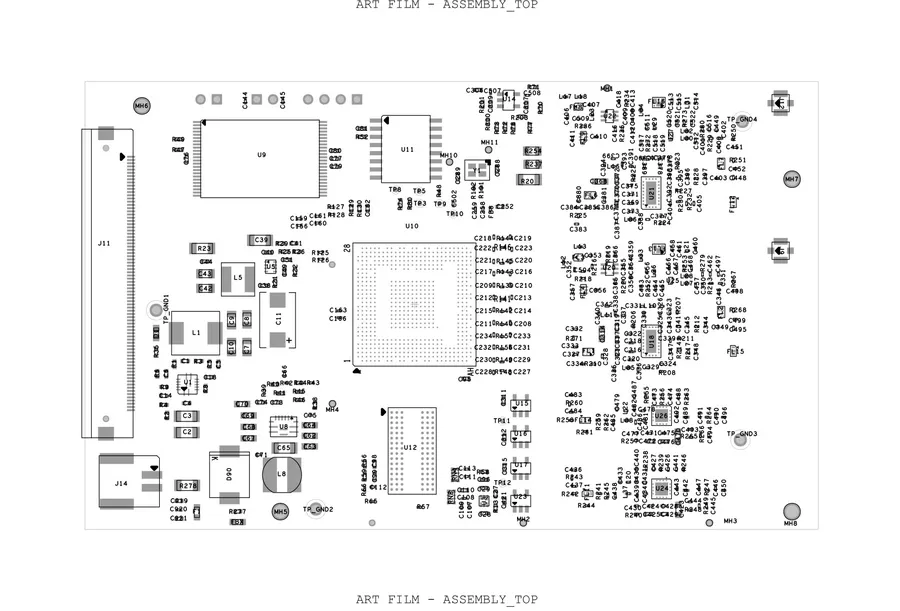
PCB assembly drawings are crucial documents that detail how components are physically placed and oriented on a printed circuit board, going beyond just the layout. These drawings serve as essential guides for the assembly process, ensuring correct component placement, which is fundamental for the proper functionality of the assembled electronic device. Accurate assembly drawings are a direct reflection of the design intent, facilitating smooth and efficient manufacturing.
These drawings are integral to ensuring quality control and avoiding costly errors in mass production, providing all the necessary details for accurate component mounting on the PCB. Furthermore, complete documentation, including a Bill of Materials (BOM), is essential for material procurement and tracking.
- Component Part Numbers
Each component on the PCB must be uniquely identified by its part number, linking it back to the Bill of Materials (BOM). This ensures that the correct components are used during assembly, preventing errors due to misidentification. - Placement Orientation
The orientation of each component (e.g., pin 1 indicator for ICs, polarity for diodes and capacitors) must be clearly marked. Incorrect orientation can cause the circuit to malfunction or damage components, so precise indication is critical. - Reference Designators
Each component on the PCB is assigned a unique reference designator (e.g., R1, C2, U3) as a label, used on both the schematic and the PCB layout, facilitating easy cross-referencing, traceability and making component identification faster on the board. - Notes for the Assembly Team
The assembly drawing includes any special instructions or notes for the assembly team, such as specific mounting instructions for certain components (e.g., heat sinks, connectors) or special soldering processes, clarifying potential points of confusion and ensuring that procedures are uniform and consistent. Additional information, such as the solder paste stencil placement for surface-mount components, might also be included. - Bill of Materials (BOM)
The BOM is a comprehensive list of all parts needed to assemble the PCB, including part numbers, quantities, manufacturers, and descriptions. It’s a vital complement to the assembly drawings, aiding in material procurement, cost estimations, and inventory control, ensuring that no needed part is missed.
Frequently Asked Questions About PCB Drawing
This section addresses common queries related to PCB drawing, providing clear and concise answers to enhance understanding and proficiency in PCB design. We aim to demystify the process and offer practical insights for both beginners and experienced designers.
- What exactly is PCB drawing?
PCB drawing refers to the creation of visual representations of a printed circuit board (PCB). This encompasses schematic diagrams, which depict the logical connections of electronic components, and layout drawings, which show the physical arrangement of these components and the conductive traces on the board. In essence, it's the blueprint that guides the fabrication and assembly of electronic circuits. - What does PCB stand for?
PCB stands for Printed Circuit Board. It is a non-conductive material, usually fiberglass or composite, with conductive pathways and pads that interconnect electronic components. The board serves as a physical support and electrical connection medium for building electronic circuits. - Is PCB design difficult to learn?
While PCB design involves several complex processes, it's not inherently difficult to learn. Like any technical skill, it requires time and effort to understand the fundamental concepts and practical application of PCB design software. Beginners can start with basic designs and gradually increase complexity. Available educational resources make it accessible to learn the necessary skills progressively. - What are PCB assembly drawings?
PCB assembly drawings are diagrams that show how components are placed on a physical PCB. These drawings specify the exact location, orientation, and part number of each component, along with other instructions to the assembly team. They are used in the manufacturing process to ensure accurate component placement during PCB assembly, acting as a guide for the automated or manual assembly process. - How do I choose the right PCB design software?
Selecting the right software depends on project complexity, budget and preferred workflows. Consider your project needs, whether you need free, open-source software or paid premium options. Features like schematic capture, layout design, and simulation should be checked. User reviews and tutorials can guide you. - What are common mistakes to avoid in PCB drawing?
Common mistakes include incorrect component placement, inadequate trace spacing, ignoring design rule checks (DRC), and neglecting thermal management. These mistakes can lead to circuit failure and manufacturing issues. Adhering to design rules and best practices is critical. - How can I improve my PCB drawing skills?
Improving PCB drawing skills involves continuous learning and practice. Start with simpler designs, gradually tackling more complex projects. Consult reliable sources, utilize software tutorials, and engage with the community to learn from other’s experiences. Design reviews by peers and iterative revisions can provide significant opportunities for improvement.
Advanced Techniques in PCB Drawing
Advanced PCB drawing involves navigating complex design challenges that go beyond basic single-layer layouts. These techniques are crucial for modern electronics requiring high performance, miniaturization, and specialized signal handling. Mastering multi-layer boards, high-speed design principles, and impedance control are essential for engineers aiming to produce cutting-edge electronic devices.
- Multi-Layer Boards
Multi-layer PCBs allow for increased circuit density and improved signal routing by stacking multiple layers of conductive material separated by insulating layers. This approach significantly reduces board size and enables the design of more complex circuits. - High-Speed Design
High-speed design focuses on managing signal integrity in circuits operating at high frequencies, where factors such as impedance matching, signal reflections, and crosstalk become critical. Proper routing and component placement are essential to ensure signal quality and prevent data corruption. - Impedance Control
Impedance control ensures consistent signal transmission by matching the impedance of traces to the impedance of components, minimizing signal reflections and maintaining signal integrity. This is crucial for high-frequency applications like RF circuits and digital data buses.
Design software plays a key role in managing these complexities, offering features like advanced routing algorithms, impedance calculators, and 3D visualization to effectively handle these challenges. Following industry standards (e.g., IPC standards) and guidelines ensures the reliability and manufacturability of these intricate designs.
| Technique | Description | Key Considerations |
|---|---|---|
| Multi-Layer PCB Design | Employing multiple conductive layers separated by insulating materials. | Layer stack-up, via placement, and routing strategy. |
| High-Speed Design | Addressing signal integrity issues in high-frequency circuits. | Impedance matching, trace routing, and component placement. |
| Impedance Control | Matching trace impedance to circuit components. | Trace width, layer spacing, dielectric materials. |
Consider the case of a high-speed data acquisition system, where controlled impedance traces are critical for accurate data transmission, or the development of a compact wearable device that utilizes multi-layer construction to achieve a smaller form factor. These advanced design requirements demand a deep understanding of PCB layout principles, software capabilities, and careful planning to guarantee the successful creation of reliable and high-performing electronic products.
Troubleshooting Common PCB Drawing Issues
Effective PCB drawing is crucial for functional and reliable electronic devices, yet it often involves encountering and resolving various design challenges. This section addresses common issues, providing practical solutions and emphasizing the importance of continuous learning to enhance design quality.
- Routing Errors
Routing errors, such as traces that are too close to each other, improperly routed traces, or missing connections, can cause shorts, open circuits, and signal integrity problems. Software design rules (DRC) can help identify these problems. Corrective actions involve adjusting trace widths, clearances, and routing paths, or using vias to change layers for better routing. - Clearance Issues
Insufficient clearance between traces, pads, and other features can result in shorts. Design rules help in identifying these issues. Resolution might involve increasing spacing between components or traces and using polygon pours to connect to the ground plane. Ensuring minimum required spacing is critical for the boards’ reliability. - Inadequate Thermal Management
Poor thermal management can lead to component overheating and potential circuit failures, particularly in high-power applications. Corrective measures include the addition of thermal vias, heat sinks, or increasing the copper area for heat dissipation. Thermal simulation tools can be used to identify hot spots and optimize thermal layout. - Component Footprint Mismatches
Incorrect component footprint can cause assembly issues or shorts. This involves checking the datasheet carefully, comparing with library symbols. If this is causing assembly issues, manually checking the footprint against a physical component is advised. - Signal Integrity Problems
Reflections, crosstalk, and electromagnetic interference (EMI) can degrade signal quality. Addressing signal integrity involves properly routing differential pairs, controlling impedance by adjusting trace widths and layer stackup, utilizing ground planes, and ensuring return paths have minimal loops. Simulation software and TDR (Time Domain Reflectometer) tools can help diagnose and solve the issue. - Design Rule Check (DRC) Failures
DRC violations indicate design issues that can lead to manufacturing problems or functional failures. To prevent them, double-check the rules and the design. This includes checking minimum distances, trace width, and component clearances. Correcting them ensures that the design is ready for manufacturing. - Manufacturing Issues
Errors in board manufacturing may arise due to poorly generated Gerber files, and/or the board does not meet the manufacturer’s design rules. To prevent issues here, communicate regularly with the manufacturer and request a DFM (design for manufacturing) check.
Effective troubleshooting utilizes diagnostic tools within PCB design software, including design rule checks (DRC), simulation capabilities, and visual inspections. Continuous learning through industry publications and manufacturer guidelines helps in avoiding common errors and optimizing designs for performance and manufacturability.
Mastering PCB drawing is crucial for anyone involved in electronics, from hobbyists to professionals. With a solid understanding of the foundational principles, appropriate tools, and a commitment to best practices, you can transform your ideas into working electronic devices. This comprehensive guide should serve as a stepping stone for your journey in PCB design. Always prioritize accuracy and quality, as these are the cornerstones of efficient, working designs. PCB drawing provides the necessary foundation to building the device, the heart of technological advancement.