Blog

PCB Plated Through Holes (PTH) vs. Vias: Concepts and Manufacturability

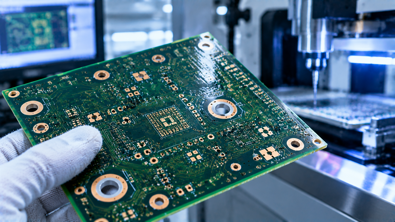
In PCB design, holes are not all created equal. Plated through holes (PTH), vias, and non-plated through holes (NPTH) serve completely different purposes. Mislabeling them in design files often leads to manufacturing delays, extra costs, or assembly failures. This guide explains the differences and the manufacturing pitfalls to avoid.
2026.10.19

What Is a Backplane PCB? Key Functions, Advantages, and Manufacturing Priorities

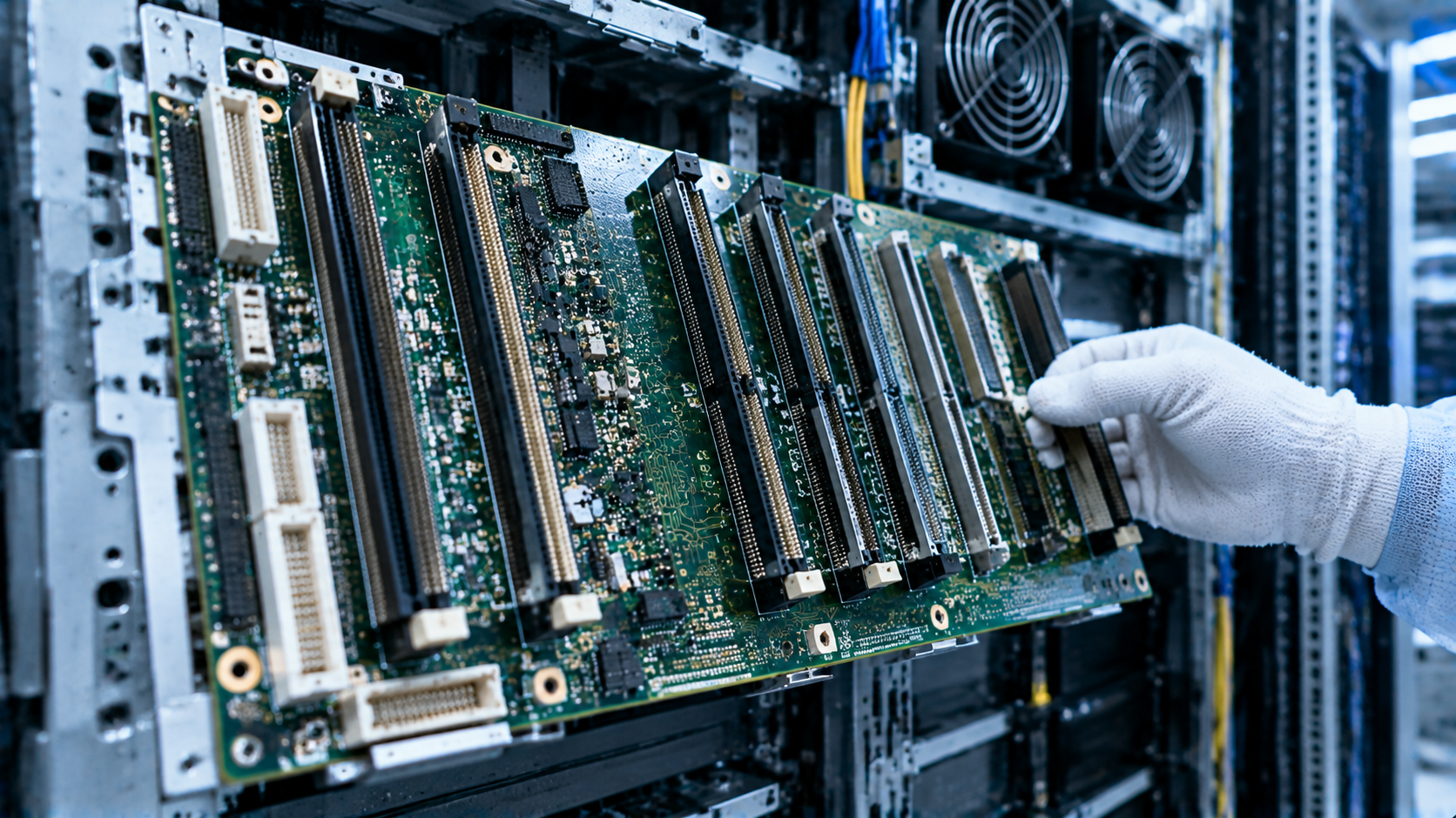
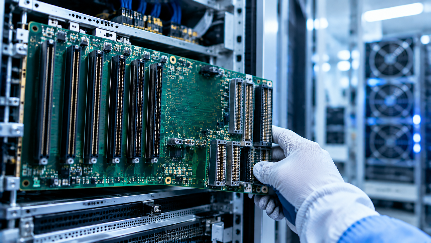
A backplane PCB sits at the back or bottom of electronic equipment, supporting and connecting multiple subsystems. Unlike standard PCBs, backplanes feature higher layer counts, more connectors, and demanding requirements for high-speed signal transmission, power distribution, thermal management, and EMI/EMC. This guide covers their core functions, key advantages, and manufacturing priorities.
2026.10.19

What Is a Backplane PCB? Key Functions, Advantages, and Manufacturing Considerations

A backplane PCB sits at the back or bottom of electronic equipment, supporting and connecting multiple components and subsystems. Unlike standard PCBs, backplanes handle higher layer counts, more connectors, and demanding requirements for signal integrity, power distribution, thermal management, and EMI/EMC. This guide covers their functions, advantages, and manufacturing priorities.
2026.10.16

LCD and Touchscreen PCB Design: From Working Principles to Manufacturability

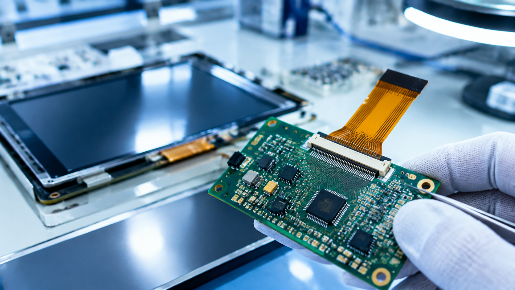
LCD and touchscreen technology is at the core of devices from smartphones to medical equipment. PCB design directly affects their performance and reliability. This guide covers signal integrity, power management, interface design (MIPI DSI, LVDS), grounding and shielding, stack-up, layout, thermal management, and serviceability.
2026.10.16

What Is HDI? PCB Design Basics and HDI Manufacturing Process

High-density interconnect (HDI) PCBs pack more components into smaller spaces using blind vias, buried vias, microvias, via-in-pad, and fine traces. This guide covers HDI design fundamentals, material selection, stack-up planning, via types, sequential lamination, metallization, and manufacturing considerations.
2026.10.15

15 Common PCB Circuit Effects Every Engineer Should Know

Some PCB problems aren't caused by design errors—they're caused by physical effects. This guide covers 15 common PCB circuit effects, from bridging and ripple to crosstalk, reflection, thermal expansion, and via effects—explaining the symptoms, root causes, and mitigation measures for each.
2026.10.15

High-Speed PCB Design Guide: From Stack-Up Planning to Signal Integrity

Most PCBs carry some risk of signal integrity problems, especially in high-speed digital designs. This guide covers high-speed PCB design fundamentals—stack-up planning, impedance control, material selection, layout strategy, routing, and power integrity—from both an engineering and manufacturing perspective.
2026.10.14

PCB Pad Types and Design Standards: A Complete Guide

Pads are the basic building blocks of surface mount assembly. They form the land pattern of a PCB and serve both electrical connection and component fixation. This guide covers common pad types—square, round, island, polygonal, oval, and open—along with special pads like thermal relief, star, and teardrop pads, and the key design standards for pad shape, size, hole diameter, and reliability.

2026.10.13

PCB Warpage and Bowing: Causes, Prevention, and Manufacturing Control

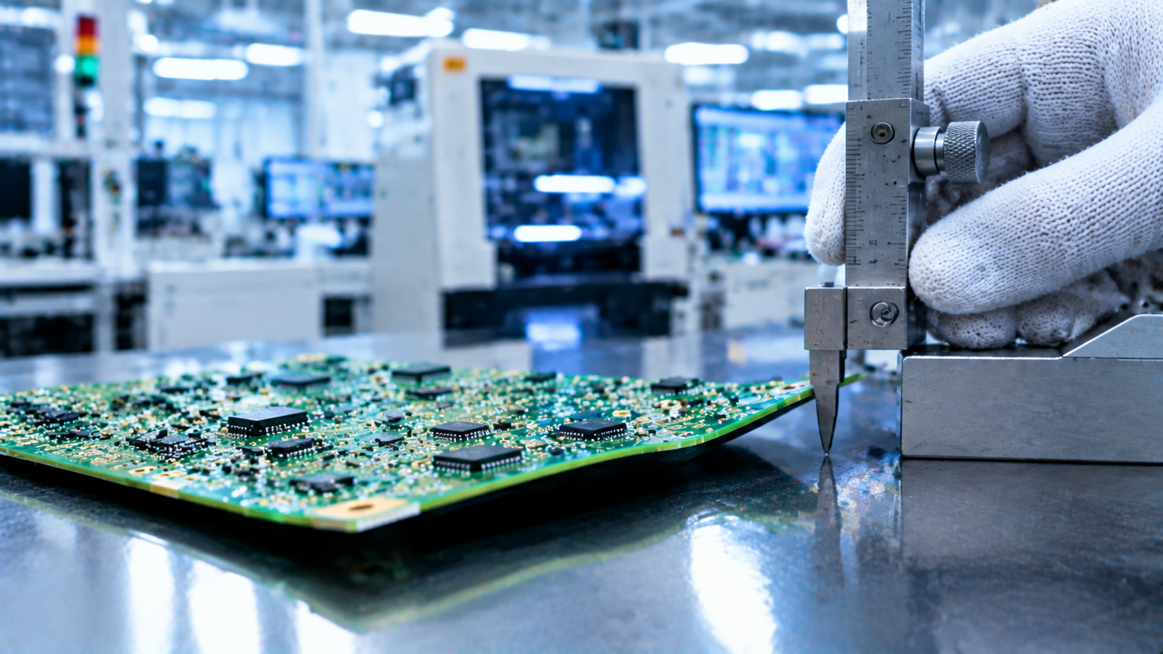
PCB warpage and bowing are among the most common hidden defects in SMT production. They can cause placement offset, poor solder joints, cracked components, and AOI failures. This article explains the causes—thermal, plating, material, design, and mechanical—and the measures to prevent them.
2026.10.13

Why Great High-Power PCB Designers Are Hard to Find

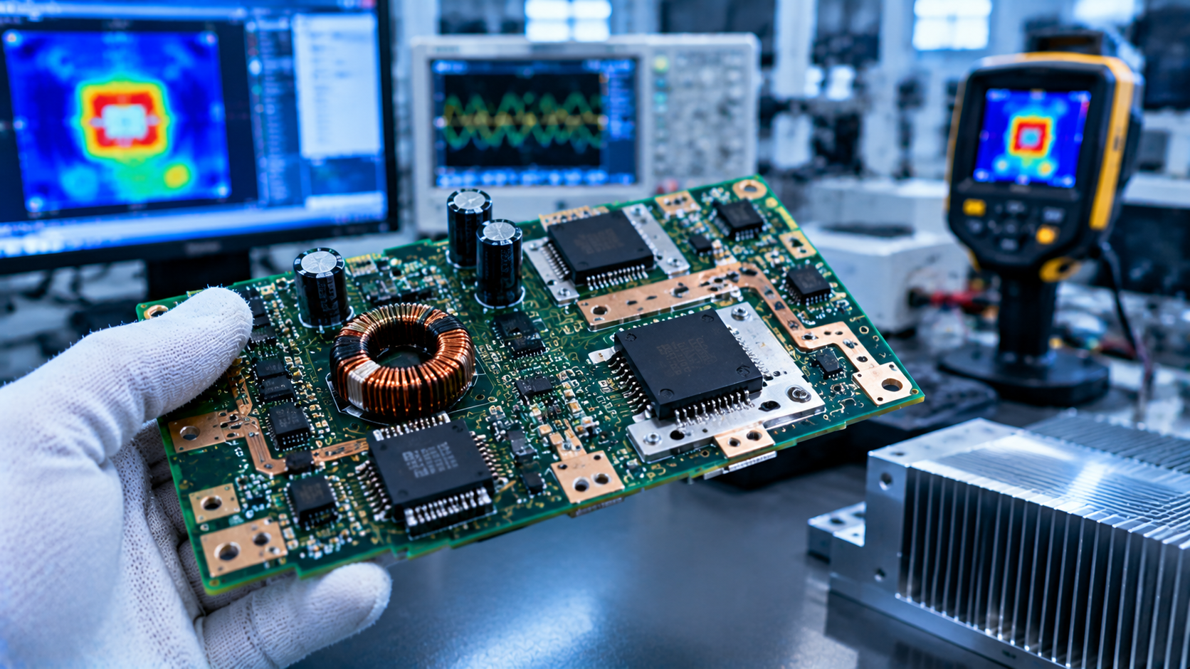
High-power PCB design is more than connecting components. It requires balancing thermal management, EMC, signal integrity, power integrity, component placement, and routing—all within tight space and cost constraints. This article explains why engineers with this combination of skills are rare, and what manufacturing-side factors they need to understand.
2026.10.13

Why 30% of Your BOM Can Be Replaced: A Manufacturer's Guide to Component Optimization

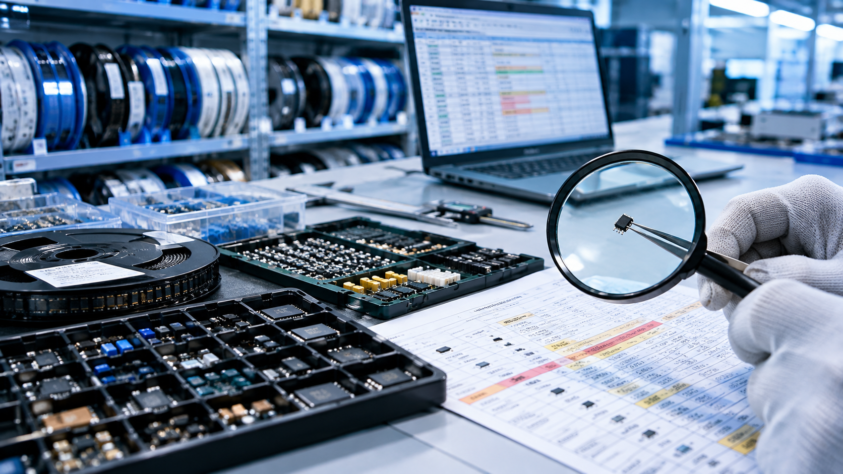
Most BOMs contain components that exceed actual design requirements—over-specified parameters, brand preferences, and packaging choices that add cost, extend lead times, and narrow supply options. This article explains where these optimization opportunities come from and how to evaluate whether a component should be replaced.
2026.10.10

PCB Terminology Every Engineer Should Know: From Stack-Up to Solder Mask

Understanding PCB terminology is essential for hardware engineers, procurement teams, and anyone communicating with manufacturers. This guide explains PCB construction—substrate, copper foil, solder mask, silkscreen—and defines the key terms used in PCB design, fabrication, and assembly.
2026.10.10