Blog

PCB Solder Mask Design Guide: From Basics to DFM Manufacturing Standards

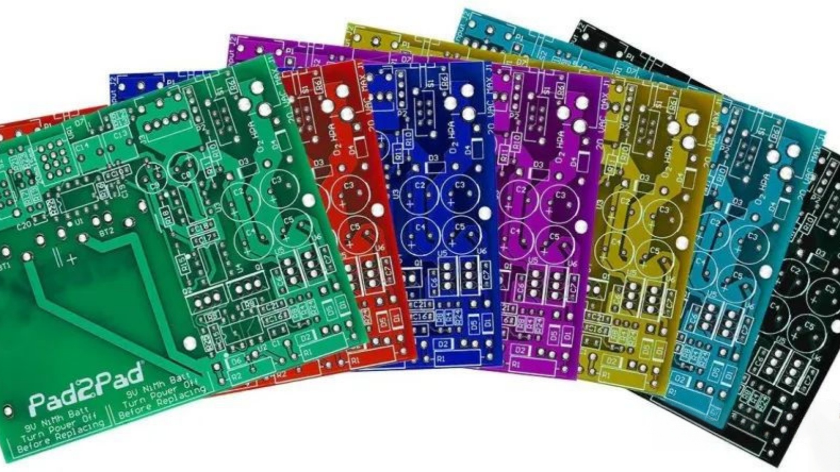
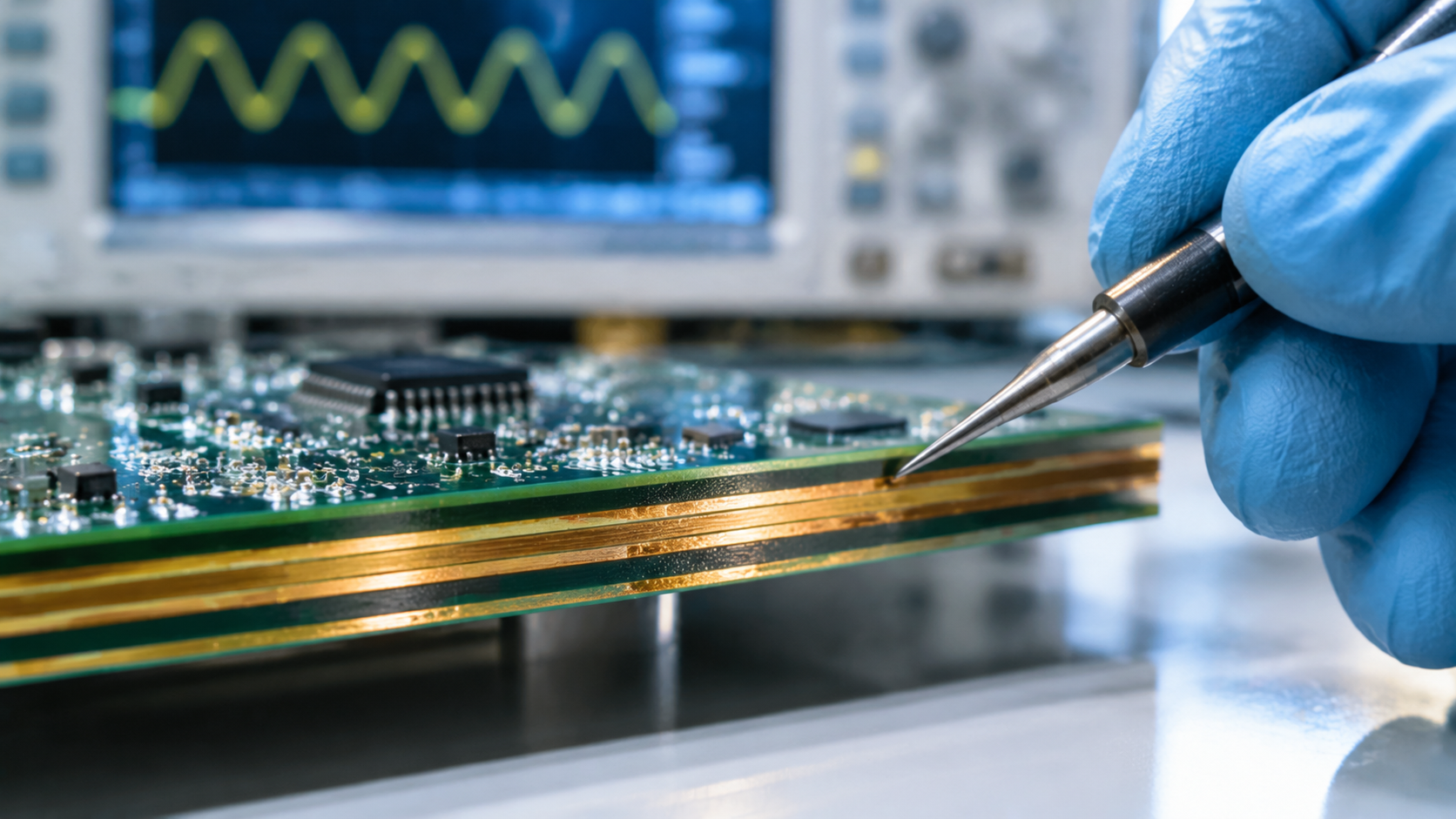
PCB solder mask (solder resist) is more than just the green coating on a circuit board—it is a critical layer that prevents solder bridging, protects copper traces from oxidation, and ensures electrical insulation. However, poor solder mask design, such as inadequate solder bridges between dense IC pins or improperly tented vias, can lead to catastrophic SMT short circuits. In this guide, AnyPCBA's engineering team breaks down the essentials of solder mask design, explains why green is the industry standard, and provides actionable DFM rules to improve your next hardware project's yield.
2026.11.12

The Unseen Half of AI: How High-End PCB Manufacturing Is Evolving

While the world focuses on 3nm chips and advanced packaging, the true foundation of the AI revolution lies hidden beneath the surface: the PCB and its material ecosystem. The PCB industry is undergoing a massive divergence, with AI-related boards growing at 45%–70% CAGR while standard boards stagnate. This article explores the shift toward 18+ layer high-end boards, the "semiconductorization" of PCBs driven by 224Gbps signal speeds, and how AnyPCBA's advanced manufacturing capabilities support next-gen AI servers and automotive electronics.
2026.11.12

Global Supply Chain Rebalancing: Why Resilience Is the New Bottom Line for Hardware Manufacturing

The global electronics supply chain is undergoing a structural reorganization. Driven by geopolitical tensions, AI-driven capacity squeezes, and component shortages, the old "lowest-cost" sourcing logic is failing. This article explores the new reality—from the "black hole effect" of high-end capacity to the need for supply chain resilience—and how agile manufacturing partnerships are becoming essential for hardware R&D teams.
2026.11.10

SMT Reflow Profile Settings: How Preheat, Soak, Reflow, and Cooling Affect Solder Joint Quality

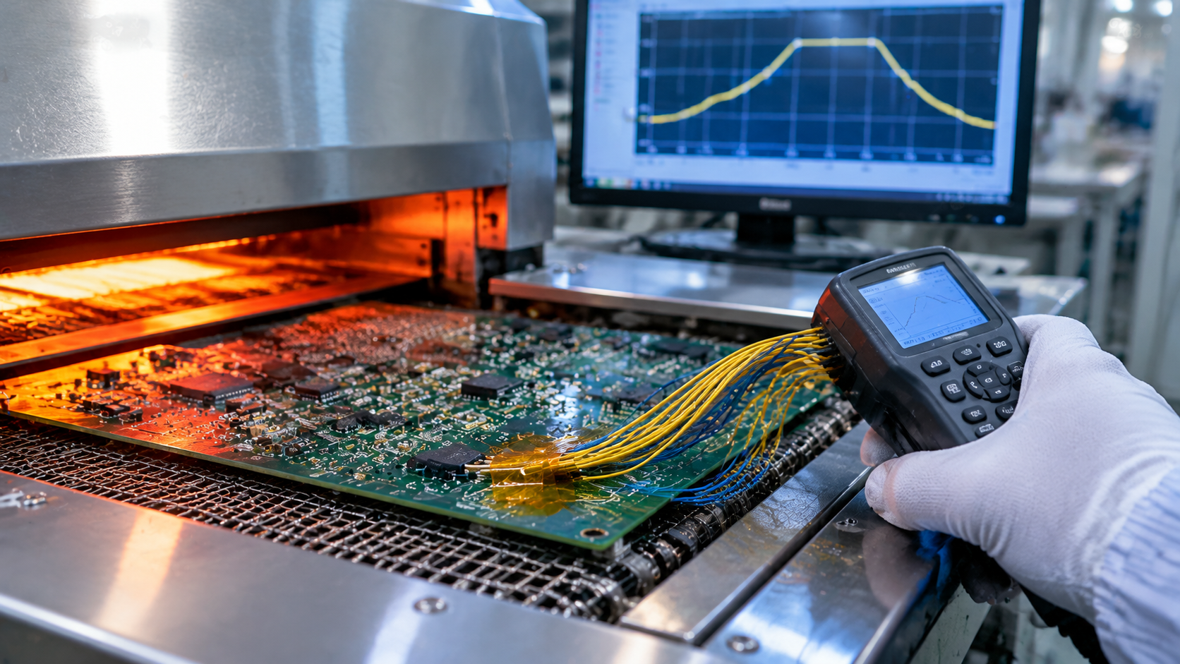
The reflow profile is one of the most critical factors in SMT assembly. It determines how solder paste melts and forms reliable joints with PCB pads and component leads. This guide breaks down the four stages of a reflow profile—preheat, soak, reflow, and cooling—and explains how each stage affects wetting, mechanical strength, and long-term reliability.
2026.11.10

How to Avoid Crosstalk in PCB Design: Layout, Routing, and Manufacturing

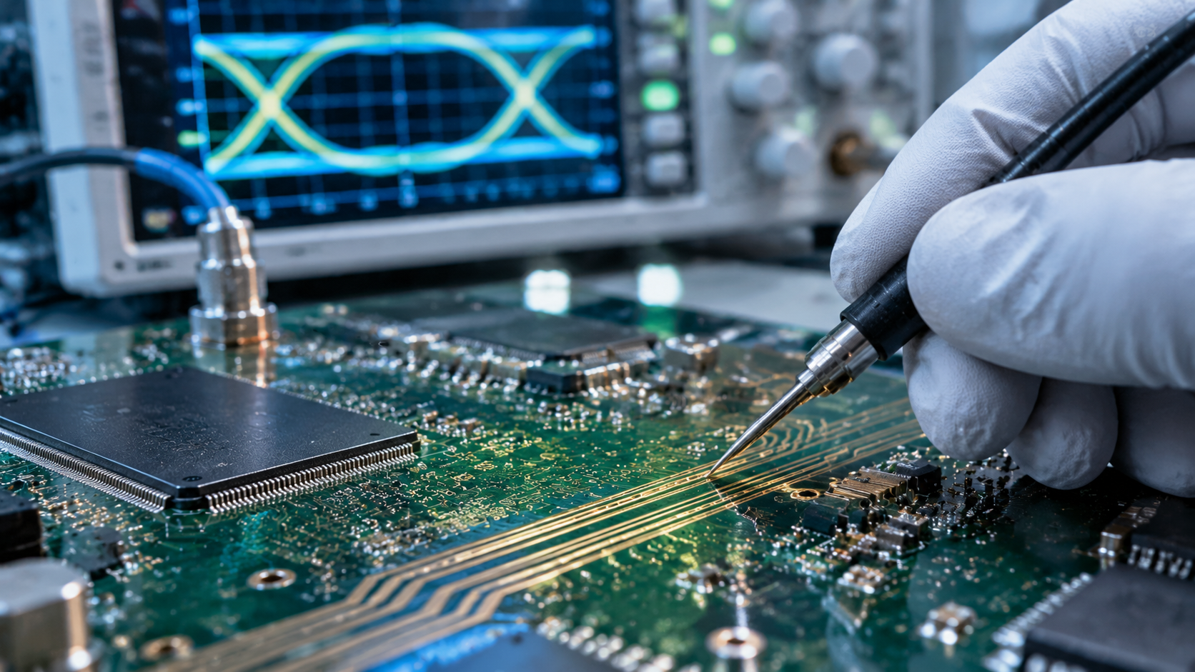
Crosstalk is one of the most common causes of signal distortion and system failure in high-speed PCB designs. It occurs when electromagnetic fields from one trace couple onto an adjacent trace. This guide covers the physical causes of crosstalk—capacitive and inductive coupling—and provides practical strategies for layout, routing, noise suppression, simulation, and manufacturing control to minimize it.
2026.11.10

How to Design PCBs for High Current: Methods and Precautions

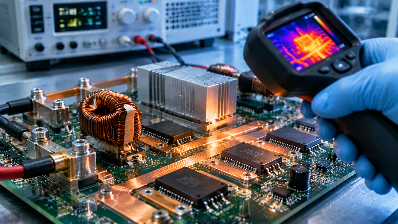
When a PCB must carry hundreds or thousands of amps, standard trace rules no longer apply. This guide covers high-current PCB design methods—heavy copper, wider traces, large copper pours, optimized layout, and thermal simulation—along with critical precautions including heat management, overcurrent prevention, insulation safety, and real-time monitoring.
2026.11.06

How to Properly Design and Route Ground (GND) on a PCB

Ground (GND) is not just a single 0V reference—it includes analog ground (AGND), digital ground (DGND), power ground (PGND), chassis ground, and earth ground. Connecting them incorrectly causes signal crosstalk, precision loss, EMC failures, and reduced system reliability. This guide explains GND classification, why blind merging fails, and three critical routing rules: proper partitioning, avoiding split GND crossings, and eliminating narrow GND bottlenecks.
2026.11.05

FPC Flexible Circuit Boards: Structure, Materials, Bend Radius, and Manufacturing

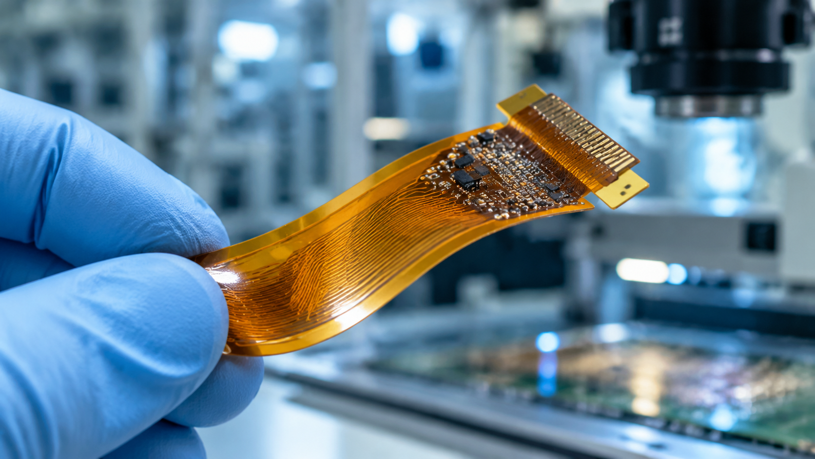
FPC (Flexible Printed Circuit) boards enable 3D routing, weight reduction, and space savings in devices like smartphones, wearables, and medical equipment. This guide covers FPC materials (PI, copper foil, coverlay, stiffeners), common structures (single-sided, double-sided, multilayer, rigid-flex), advantages and limitations, and the critical bend radius calculation that prevents copper fatigue and delamination.

2026.11.05

The Complete PCB Design Workflow: From Concept to Mass Production

A successful electronic product requires more than a schematic. It needs rigorous layout, stack-up planning, routing, and a seamless transition to manufacturing. This guide covers the seven core stages of the PCB design workflow—from requirements analysis and schematic capture to layout, routing, DRC, and fabrication outputs—plus outsourcing best practices and DFM review.
2026.11.04

Solder Paste vs. Red Glue in SMT: Process Selection and Manufacturing Trade-offs

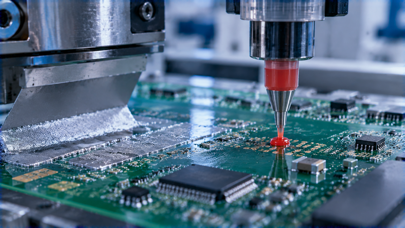
In SMT assembly, solder paste and red glue (SMT adhesive) serve different purposes—one creates the electrical and mechanical solder joint, the other simply holds components in place. Choosing the right process—or combining both—directly affects cost, yield, and reliability. This guide compares the two processes, explains their applications and limitations, and provides selection criteria for mixed SMT/DIP assembly.
2026.11.04

Multilayer PCB Structure: How to Increase Routing Density and Performance

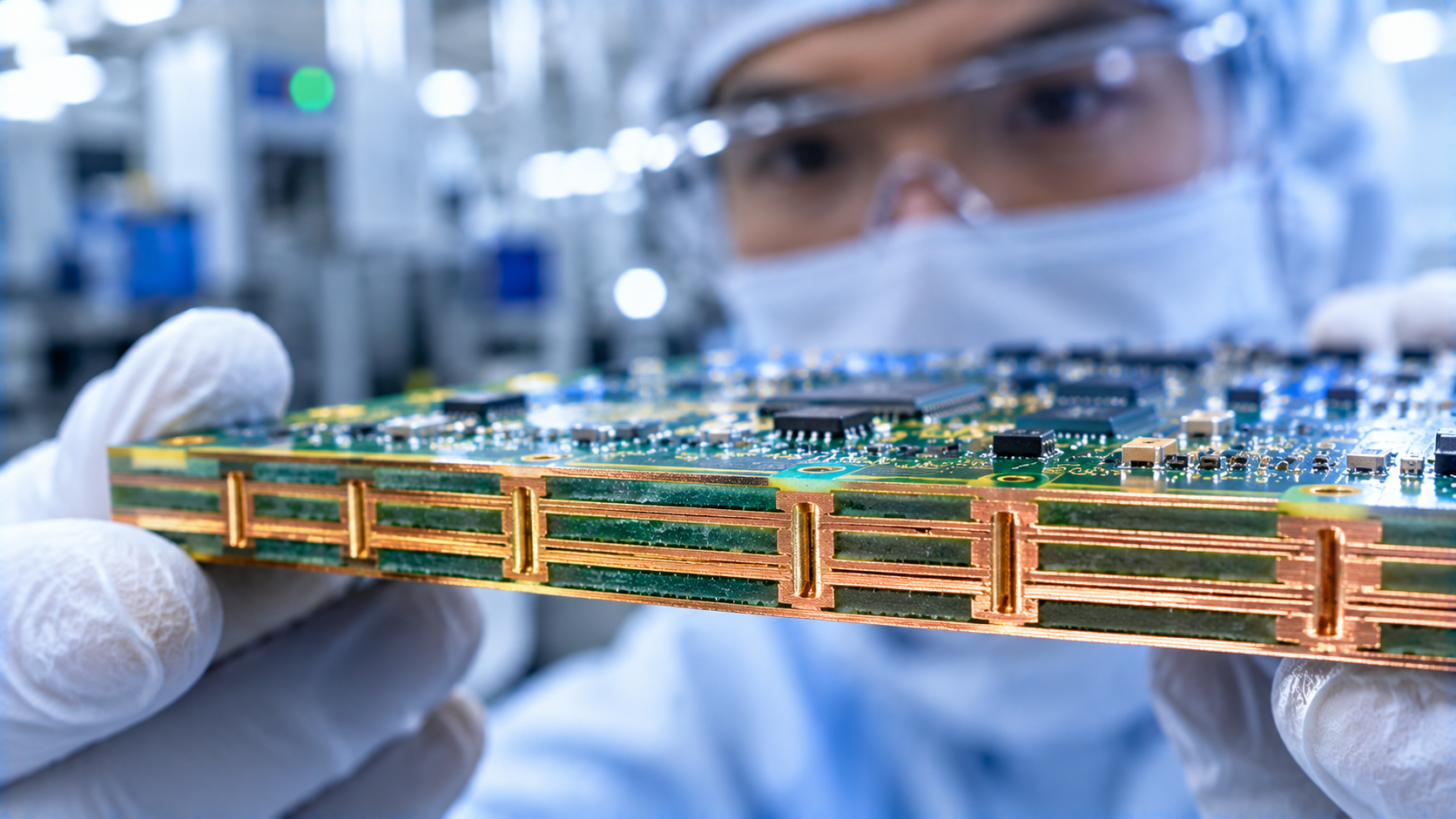
Multilayer PCBs stack alternating layers of copper and insulating material, using vias to connect them in three dimensions. This guide covers the basic structure of multilayer boards, four methods to increase routing density—adding layers, optimizing via design, using finer traces, and adopting high-density packaging—and the core advantages they deliver in size, speed, performance, and cost.
2026.11.03

The 2026 AI Hardware Boom: Reshaping the Global PCB Supply Chain

The AI boom is pushing power consumption past 1,000W per chip and driving the shift to Chiplets and high-speed materials. This article explores how these demands are reshaping global PCB manufacturing—from 20oz heavy copper and Any-layer HDI to high-frequency hybrid laminates—and why agile, small-to-medium batch manufacturing is becoming the backbone of global hardware innovation.
2026.11.03